

Panasonic AN3117SA, AN3117S Datasheet
Other ICs for Video
AN3117S, AN3117SA
RF modulator IC for VCR and VDP
■ Overview
The AN3117S and AN3117SA are RF modulator ICs
for VCR and VDP. They provide excellent high frequency
characteristics by adopting the high performance RF oscillation circuit.
■ Features
• Excellent in higher harmonic characteristics of RF
• Excellent in higher harmonic characteristics of sound
sub-carrier by the 1 MIX system
• Sharp white clip characteristics
• Suitable RF-MOD IC for the USA and Japan specifica-
tions
• Video AM modulator
• RF carrier oscillator
• White clip
• Channel changeover SW
• Sound FM modulator
• ANT SW driver
• Carrier off SW
• Available also the SSOP package (0.65 mm pitch)
■ Applications
• Video deck, video disk player, set top box for CATV,
game machine
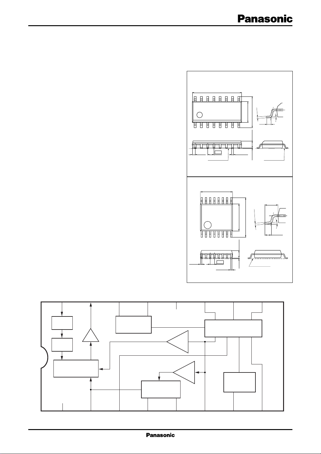
■ Block Diagram
4.2±0.3
6.5±0.3
0.1±0.1 1.5±0.2
Unit: mm
(0.15)
0.3
AN3117S
10.1±0.3
16 9
18
1.27
(0.605)
Seating plane Seating plane
0.40±0.25
SOP016-P-0225A
AN3117SA
5.0±0.2
16
18
(0.225)
0.22
0.65
+0.10
− 0.05
9
4.4±0.2
6.4±0.3
1.2±0.20.1±0.1
Unit: mm
−0.05
+0.10
0.15
Seating plane
SSOP016-P-0225A
(0° to 10°)
(1.0)
0° to 10°
0.5±0.2
16
Video
clamp
White
clip
1
Video in
MIX
GND
15
Buff.
2
RF out
P/S Adj.
14
3
ANT SW
driver
13
mod.
4
12
RF
amp.
FM
5
11
Pre
amp.
6
Audio in
10
RF
OSC
Channel
SW
7
9
8
1
AN3117S, AN3117SA Other ICs for Video
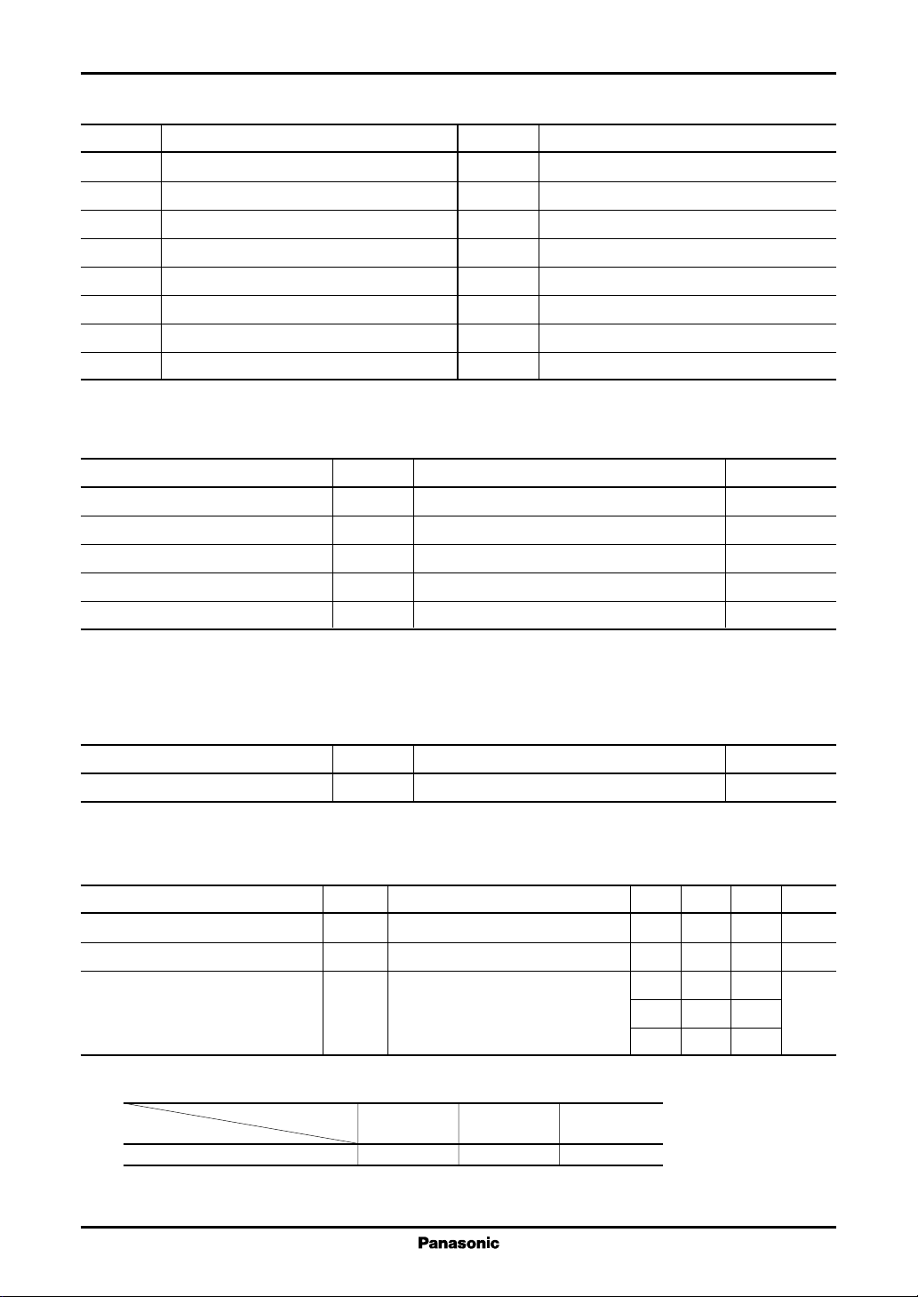
■ Pin Descriptions
Pin No. Description
1 Ground pin
2 P/S adjustment pin
3 RF OSC control pin
4 SIF oscillation pin 1
5 SIF oscillation pin 2
6 Sound input pin
7 Channel changeover pin
8 SAW/LC oscillation changeover pin
■ Absolute Maximum Ratings
Parameter Symbol Rating Unit
Supply voltage V
Supply current I
2
Power dissipation
Operating ambient temperature
Storage temperature
Note)*1: Except for the operating ambient temperature and storage temperature, all ratings are for Ta = 25°C.
2: The power dissipation shown is for the IC package in free air at Ta = 75°C.
*
*
1
*
1
*
CC
CC
P
D
T
opr
T
stg
Pin No. Description
9 RF oscillator emitter pin 1
10 RF oscillator emitter pin 2
11 RF oscillator base pin
12 Power supply pin
13 Antenna switch driver changeover pin
14 Antenna switch driver pin
15 RF output pin
16 Video input pin
6V
60 mA
269 mW
−20 to +75 °C
−55 to +150 °C
■ Recommended Operating Range
Parameter Symbol Range Unit
Supply voltage V
CC
4.5 to 5.5 V
■ Electrical Characteristics at VCC = 5 V, Ta = 25°C
Parameter Symbol Conditions Min Typ Max Unit
Current consumption ITOT
Video output level VP No video and sound input 83 85 87 dBm
1
Video modulation depth
Note) 1. Measure in USA 3-ch. unless otherwise specified.
2.*1: Video modulation coefficient ranks.
Sound modulation coefficient
23 kHz to 27 kHz B C D
• Normal delivery for B to D ranks with embossed taping of 2 000 pcs per reel
• The rank can not be specified in your order.
*
Video modulation coefficient
mV Video input = 0.625 V[p-p] 73 79 %
2
VCC = 5 V, no video and sound input
18 22 26 mA
10-staircase wave 77 80 83
81 87
73% to 79% 77% to 83% 81% to 87%
Other ICs for Video AN3117S, AN3117SA
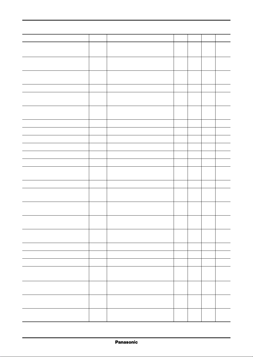
■ Electrical Characteristics at VCC = 5 V, Ta = 25°C (continued)
Parameter Symbol Conditions Min Typ Max Unit
Video output difference between ∆V
No video and sound input −20 2dB
P
channels
Video modulation coefficient ∆m
Video input = 0.625 V[p-p] −20 2 %
V
difference between channels 10-staircase wave
Maximum video modulation m
Video input = 1.0 V[p-p] 88 93.5 97 %
Vmax
coefficient 10-staircase wave
P/S ratio V
Sound modulation coefficient f
No video and sound input 9.5 12 14.5 dB
PS
Sound input = 245 mV[rms] 23 25 27 kHz
∆FM
f = 1 kHz, sine wave
Maximum sound modulation f
∆Fmax
coefficient f = 1 kHz, ratio with f
Sound S/N SN
Sound input = 980 mV[rms] 3.6 4 4.4
∆FM
No video input 55 63 dB
S
Sync. distortion Sync m = 80% Full white signal −2.5 %
Differential gain DG m = 80% Staircase wave 3 %
Differential phase DP m = 80% Staircase wave 2 deg
Sound modulation distortion THD f
Sound oscillation frequency f
SIF
Driver output voltage ASV V
= ±25 kHz 0.3 %
∆FM
VCC = 5 V 4.50 MHz
= 5 V, 13-pin open 0 V
CC
at ANT SW on RF carrier off
At ANT SW off ASRV VCC = 5 V, 13-pin 5 V 4.0 V
Driver output voltage RF carrier on
Load current 15 mA
ANT SW COFF V
= 5 V 0.25 V
CC
RF carrier off voltage
ANT SW CON V
= 5 V 1.25 V
CC
RF carrier on voltage
Chroma beat IM P/S = 12 dB, P/C = 18 dB, 65 dB
P = 66 dBµ, 3.58 MHz, sine wave
In-band beat Beat 70 dB
Video input impedance R
Sound input impedance R
Video output level ∆V
V
A
PTTa
= 25°C reference ±2dB
30 kΩ
20 kΩ
Temperature characteristics Ta = −10°C to +70°C
Video modulation coefficient ∆m
Ta = 25°C reference ±3 %
T
Temperature characteristics Ta = −10°C to +70°C
Maximum video modulation coefficient
∆m
maxTTa
= 25°C reference 87.5 %
Temperature characteristics Ta = −10°C to +70°C
Sound oscillation ∆f
Ta = 25°C reference ±10 kHz
ST
Frequency stability Ta = −10°C to +70°C
Note) Measure in USA 3-ch. unless otherwise specified.
3
 Loading...