

Panasonic AN2493FH Datasheet
ICs for VCR
AN2493FH
Luminance and chrominance signal processing (PAL) IC
for 8 mm VCR
■ Overview
The AN2493FH is a single chip LSI designed for a Y/
C main signal processing of PAL system normal 8 mm
video. System cost can be cut down drastically by builtin of external filters and fc automatic adjustment.
■ Features
• 5 V single power supply
• Reduction of external components and adjustment parts
by adopting of automatic adjustment filters.
• No need of glass delay lines.
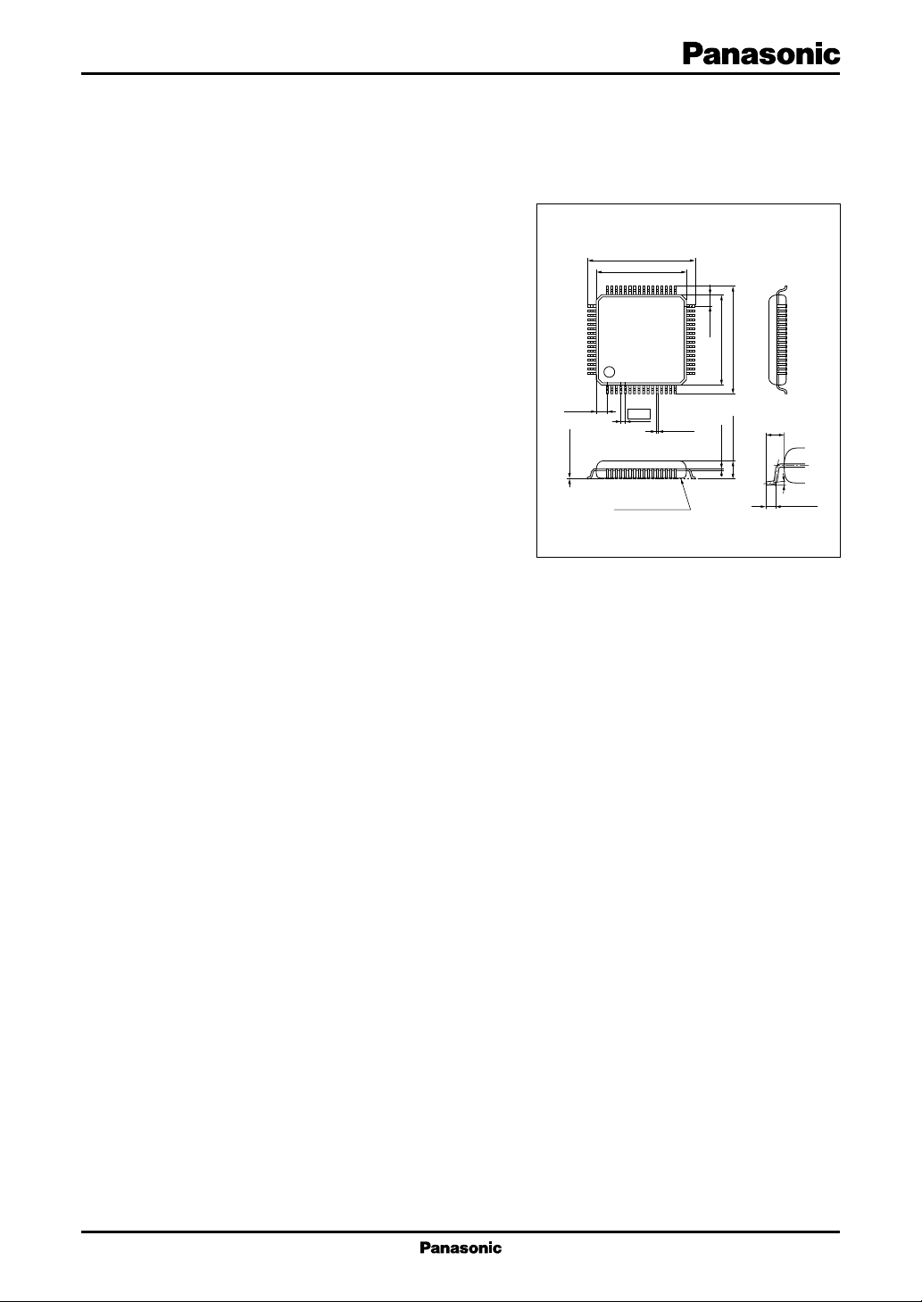
49
64
(1.25)
0.10±0.10
12.00±0.20
10.00±0.20
48 33
0.50
0.18
Seating plane
161
+0.10
−0.05
Unit: mm
32
(1.25)
10.00±0.20
12.00±0.201.95±0.20
17
(1.00)
−0.05
+0.10
0.15
0° to 10°
0.50±0.20
■ Applications
• 8 mm videos and 8 mm video cameras
QFP064-P-1010
1
AN2493FH ICs for VCR
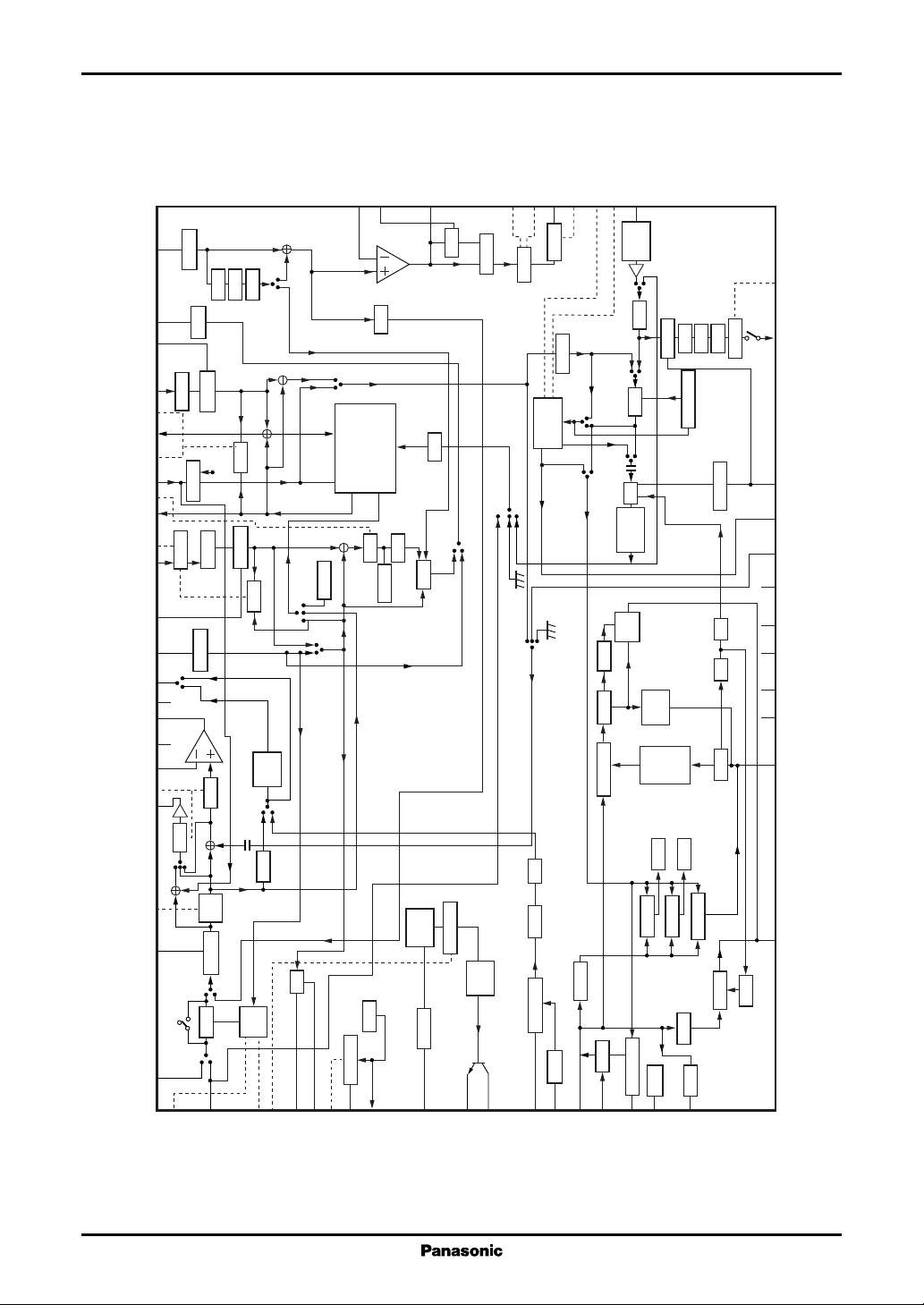
■ Block Diagram
CTL
0
DEV CTL
FM out
(DOC)20GCA3 CTL
C. E. CTL
HPF1
SW15
P
R
P
90PS
64
VXO out
19
R
SW16
1/8
1/46
Sub BM
VXO
1
VXO in
18
CEC det.17PB C in
LPF
C sub
P
R
SW13
LPF
P
R
SW14
ACC
P
R
SW17
BM
Burst
DE/EM
SLD
REC
AFC
f PC
DP PC
REF
REC APC
V
2
3
det.
REF
V
REC APC det.
CACC
4DIV
CK PC
LPF
Trap
ACC det.
CK
PB APC
1/4
DL
4
out
SC
f
HPF
GCA4
CL det.
4R
1/4
VCO
f det.
1/8
16
CK
15
14
13
12
11
10
9
8
7
6
5
GCA4 CTL
REC C out
CL CA
det.
PB C out
C MIX in
C GND
Data
CK
C V
CC
PG in
PB APC
det.
f det.
NL in
LNC out
CCL det.
CDL in
G1 det.
ADD out
GCA1 CTL
CONP C
LIMC
To CCD
G2 det.
YDL in
YCL det.
CL in
ML out
Y GND
Video out
Y V
VNF
VF mute CTL
VF out
(BGP out)
V mute CTL
Clamp det.
Line in
ME NF25W CTL24ME out
26
27
Clamp
HPF
LIM
HSS
R
P
SW12
28
Amp.
29
30
GCA1
Clamp
31
SUB2
SW8
32
33
Mute
V mute
CTL
Det.
C
34
35
CNR
36
37
38
Trap
GCA2
39
40
Clamp
PS
41
42
SW4
NOR
43
44
CC
Clamp
DET
A
CONP
SW6
PB
DOC
N
LIM
Sync.
Line
SW5
NC
ATT
CORR
(COR det. out)23f
B
BPF
MIX
(d)
W/D
P
R
SW11
Smear
SW18
R
22
MOD
P
CONP
SW2
21
GCA3
DE/EM
Chroma
PB
Line
45
Main
46
47
OSDOSD
OSD
SW1
LPF
SW3
P
R
C
ATT
PBY
DL
48
LIM
49
Main
DEMOD
Amp.
Clamp
50
SW0
SW21
51
AGC det.
R
AGC
SW19
52
CONP Y
det.
AGC
REC PB
SS
DOC
DLIM
RF AGC
54
555657
53
SS det.
VOL
SS out
RF det.
58
FM in
RF out
59
DLIM in
P
Test9
60
MDE
Sub
LPF
61
MDC
D clamp
62
63
DCL in
Clip
Clip in
2
ICs for VCR AN2493FH
■ Pin Descriptions
Pin No. Description
1 VXO in
2 REC APC det.
3V
4f
SC
REF
det.
out
5 f det.
6 PB APC det.
7 PG in.
8C V
CC
9CK
10 Data
11 C GND
12 C MIX in
13 PB C out
14 CL CA det.
15 REC C out
16 GCA4 CTL
17 PB C in
18 CEC det.
19 Chroma emph. CTL
20 GCA3 CTL
21 FM out (DOC)
22 DEV CTL
23 f0 CTL
24 ME out (COR det. out)
25 W CTL
26 ME NF
27 NL in
28 LNC out
29 CCL det.
30 CDL in
31 G1 det.
32 ADD out
Pin No. Description
33 GCA1 CTL
34 CONP C
35 LIMC
36 To CCD
37 G2 det.
38 YDL in
39 YCL det.
40 CL in
41 ML out
42 Y GND
43 Video out
44 Y V
CC
45 VNF
46 VF mute CTL
47 VF out (BGP out)
48 V mute CTL
49 Clamp det.
50 Line in
51 AGC det.
52 CONP Y
53 REC PB VOL
54 SS det.
55 SS out
56 RF det.
57 FM in
58 RF out
59 DLIM in
60 MDE
61 MDC
62 DCL in
63 Clip in
64 VXO out
3
AN2493FH ICs for VCR
■ Absolute Maximum Ratings
Parameter Symbol Rating Unit
Supply voltage V
Supply current I
2
Power dissipation
Operating ambient temperature
Storage temperature
Note)*1: Except for the power dissipation, operating ambient temperature and storage temperature, all ratings are for Ta = 25°C.
2: The power dissipation shown is for the IC package at Ta = 70°C.
*
PD = 696 (mW) (Ta = 70°C) when mounted on the glass epoxy printed circuit board of 50 × 50 × 0.8 (mm3).
3: It becomes = 471(mW) at supply voltage VCC = 4.8 V.
*
*
*1, *
1
*
CC
CC
P
D
3
T
opr
T
stg
■ Recommended Operating Range
Parameter Symbol Range Unit
5.5 V
100 mA
359 mW
−10 to +70 °C
−55 to +125 °C
Supply voltage V
CC
4.7 to 5.2 V
■ Electrical Characteristics at VCC = 4.8 V, Ta = 25°C
Parameter Symbol Conditions Min Typ Max Unit
Consumption current 1 I
Consumption current 2 I
Consumption current 3 I
Consumption current 4 I
Internal reference voltage source V
REC overall V
Y-AGC control characteristics ∆V
Y-AGC through mode V
View finder amp. f
frequency characteristics at input of 100 kHz or 5 MHz
Video-OSD V
white mute level
Video-OSD V
black mute level
Video-OSD V
white mute CTL voltage character
Video-OSD V
black mute CTL voltage character
Video-OSD V
through CTL voltage character
Consumption current at recording 52 72 92 mA
CC1
Consumption current at playback 58 78 98 mA
CC2
Power save mode 42 62 82 mA
CC3
Camera power save mode −8 −4.2 −1mA
CC4
Pin 3 voltage 2.5 V
REF
Adjust pin 47 output voltage to −14 −12 −10 dB
ME
1 V[p-p] at pin 53
Pin 47 output gain ratio between −1.5 0 1.5 dB
AGC
0.5 V[p-p] and 2.0 V[p-p] inputs
Pin 24 output at pin 50 input 200 250 300 mV[p-p]
26S
Output ratio of 5 MHz to 100 kHz −1.5 0 1.5 dB
BA
DC voltage referred to pedestal level 56 68 80 IRE
OW
DC voltage referred to pedestal level −5 5 15 IRE
OB
Pin 48 input at inserting recording 3.6 4.8 V
48W
Pin 48 input at inserting recording 2.0 2.6 V
48B
Pin 48 input at inserting recording 0 1.0 V
48S
4
ICs for VCR AN2493FH
■ Electrical Characteristics at Ta = 25°C (continued)
Parameter Symbol Conditions Min Typ Max Unit
Video-OSD quasi-V level V
Video-OSD quasi-V V
mute CTL voltage
Video-OSD V
through CTL voltage
Y-main-LPF ∆f
frequency characteristics 1 at input of 100 kHz or 3 MHz
Y-main-LPF ∆f
frequency characteristics 2 at input of 100 kHz or 4.43 MHz
Video amp. output amplitude V
Video amp. f
frequency characteristics at input of 100 kHz or 5 MHz
View finder OSD-white V
mute level
View finder OSD-black V
mute level
View finder OSD-white V
mute CTL voltage is inserted
View finder OSD-black V
mute CTL voltage is inserted
View finder OSD V
through CTL voltage is inserted
View finder OSD quasi-V level V
View finder OSD quasi-V V
mute CTL voltage
View finder OSD V
through CTL voltage
PB OSD white mute level V
PB OSD black mute level V
PB OSD white V
mute CTL voltage is inserted
PB OSD black V
mute CTL voltage is inserted
PB OSD through CTL voltage V
PB OSD off V
DC voltage difference referred to −50 0 50 mV
OV
sync. tip in PB mode
Pin 48 input in PB mode 2.0 4.8 V
48V
Pin 48 input in PB mode 0 1.0 V
48G
Output ratio of 3 MHz to 100 kHz −5 −12 dB
ML1
Output ratio of 4.43 MHz to 100 kHz
ML2
Adjust the VF out to 1 V[p-p] 1.75 2.0 2.25 V[p-p]
VO
Output ratio of 5 MHz to 100 kHz −1.5 0 1.5 dB
VI
DC voltage referred to pedestal level 56 68 80 IRE
BOW
DC voltage referred to pedestal level −5 5 15 IRE
BOB
Pin 48 = 0 V, an indication character 3.6 4.8 V
46W
Pin 48 = 0 V, an indication character 2.0 2.6 V
46B
Pin 48 = 0 V, an indication character 0 1.0 V
46S
DC voltage referred to sync. tip at −50 0 50 mV
BOV
−25 dB
PB mode
Pin 48 input in PB mode 2.0 4.8 V
B48V
Pin 48 input in PB mode 0 1.0 V
B48S
DC voltage referred to pedestal level 56 68 80 IRE
POW
DC voltage referred to pedestal level −5 5 15 IRE
POB
Pin 48 = 0 V, an indication character 3.6 4.8 V
46W
Pin 48 = 0 V, an indication character 2.0 2.6 V
46B
Pin 48 = 0 V, an indication character 0 1.0 V
46S
is inserted
Pin 48 = 0 V, an indication character 1.75 2.0 2.25 V[p-p]
VOO
is inserted
5

AN2493FH ICs for VCR
■ Electrical Characteristics at Ta = 25°C (continued)
Parameter Symbol Conditions Min Typ Max Unit
Sync. separation min. input V
sensitivity
Sync. separation pulse delay t
amount pin 40 and pin 55
Sync. separation output V
amplitude 1
Sync. separation output V
amplitude 2
Non linear emphasis 1 f
Non linear emphasis 2 f
Non linear emphasis 3 f
Non linear de-emphasis 1 f
Non linear de-emphasis 2 f
Non linear de-emphasis 3 f
RNL1
RNL2
RNL3
PNL1
PNL2
PNL3
Dark clip level V
White clip level V
FM carrier interleave V
FM modulator oscillation frequency
FM modulator deviation CTL f
DEV
FM modulator second harmonic 2f
distortion
Y-FM-GCA output amplitude 1 V
Y-FM-GCA output amplitude 2 V
PB-Y-RFAGC output amplitude V
PB-Y-RFAGC output second 2f
harmonic distortion
PB-over-all 1 (NOR) V
FM demodulation linearity 1 ∆V
Input sync. level 65 mV[p-p]
SS
Sync. delay measurement between 560 760 960 ns
SS
Output amplitude of pin 55 4.0 V
SSH
Output amplitude of pin 55 0.4 V
SSL
Output ratio of 1 MHz to 10 kHz 1.0 3.0 5.0 dB
at input 0 dB
Output ratio of 1 MHz to 10 kHz 3.7 6.2 8.7 dB
at input −10 dB
Output ratio of 1 MHz to 10 kHz 6.3 9.3 12.3 dB
at input −20 dB
Output ratio of 1 MHz to 10 kHz −5.0 −3.0 −1.0 dB
at input 0 dB
Output ratio of 1 MHz to 10 kHz −10 −7.5 −5.0 dB
at input −10 dB
Output ratio of 1 MHz to 10 kHz −11.5 −8.5 −5.5 dB
at input −20 dB
Fixed 90 100 110 %
CD
Adjust at pin 25 220 %
CW
Apply voltage to pin 7 1.64 mV[p-p]
CI
f
Adjust at pin 23 4.2 MHz
0
Apply voltage to pin 27 and adjust 2.4 MHz/V
at pin 22
Pin 21 output −30 dB
FM
Pin 20 = 0 V 100 mV[p-p]
FMS
Pin 20 = 4.8 V 370 mV[p-p]
FML
Input 50 mV[p-p] and 200 mV[p-p] 325 400 475 mV[p-p]
58
at f = 5 MHz
Input 100 mV[p-p], f = 5 MHz −30 dB
58
Adjust pin 47 output voltage at pin 53 1.0 V[p-p]
NOR
Adjust at pin 53, input 3, 5 and 7 MHz,
NOR
90 100 110 %
pin 63 = 4.8 V
6

ICs for VCR AN2493FH
■ Electrical Characteristics at Ta = 25°C (continued)
Parameter Symbol Conditions Min Typ Max Unit
Dropout detection on level V
Dropout detection off hysteresis ∆V
Dropout detection ENV off V
DOCH
Dropout detection output V
high-level
Dropout detection output V
low-level
Noise canceller frequency f
NC11
characteristics 1 at input 0 dB, NC1 mode
Noise canceller frequency f
NC12
characteristics 2 at input −10 dB, NC1 mode
Noise canceller frequency f
NC13
characteristics 3 at input −20 dB, NC1 mode
Noise canceller frequency f
NC14
characteristics 4 at input −30 dB, NC1 mode
NC off mode f
NCOFF
Clip comp. limiter level V
Line noise canceller frequency f
LNC1
characteristics 1
Line noise canceller frequency f
LNC2
characteristics 2
Line noise canceller (off) f
C-BPF frequency characteristics 1
C-BPF frequency characteristics 2
C-BPF frequency characteristics 3
C-BPF+HPF frequency
LN3
f
f
f
f
characteristics 4
REC APC pull-in range 1 +∆f
REC APC pull-in range 2 −∆f
Xtal output amplitude V
Xtal oscillation frequency f
Input at pin 57, f = 5 MHz −17 −12 −7dB
DOC
Input at pin 57, f = 5 MHz 1 4 10 dB
DOC
Input at pin 57, f = 5 MHz 5 8 11 H
Pin 21 output, pin 57 input 2.8 V
P21H
Pin 21 output, pin 57 input 0.4 V
P21L
Output ratio of 1 MHz to 50 kHz −3 − 0.3 0.5 dB
Output ratio of 1 MHz to 50 kHz −3.5 − 0.8 0.5 dB
Output ratio of 1 MHz to 50 kHz −6 −2.3 0 dB
Output ratio of 1 MHz to 50 kHz −10 −6.5 −3.0 dB
Output ratio of 1 MHz to 50 kHz at −10 −6.5 −3.0 dB
input −30 dB, NC1 mode and NC off
Pin 41 output, pin 63 input 45 70 95 mV
CL
Input 0 dB −2.2 − 0.2 1.8 dB
Input −30 dB −15.0 −8.5 −3.0 dB
Input −30 dB −1.5 0 1.5 dB
Output ratio of 4.13 MHz to −2.5 − 0.5 1.5 dB
BP1
4.43 MHz at input 100 mV[p-p]
Output ratio of 4.73 MHz to −2.5 − 0.5 1.5 dB
BP2
4.43 MHz at input 100 mV[p-p]
Output ratio of 2.93 MHz to −20 dB
BP3
4.43 MHz at input 100 mV[p-p]
Output ratio of 5.93 MHz to −18 dB
BP4
4.43 MHz at input 100 mV[p-p]
Pin 4 output (designated Xtal), 275 Hz
SC
at input fSC +300 Hz
Pin 4 output (designated Xtal), −275 Hz
SC
at input fSC −300 Hz
Pin 4 output at lock (designated Xtal) 320 520 720 mV[p-p]
FSC
Frequency deviation of pin 4 at PB −50 50 Hz
SC
7

AN2493FH ICs for VCR
■ Electrical Characteristics at Ta = 25°C (continued)
Parameter Symbol Conditions Min Typ Max Unit
ACC output amplitude V
ACC control characteristics ∆V
ACC maximum gain V
C ACC output characteristics V
Burst emphasis amount V
Burst de-emphasis amount V
Chroma de-emphasis V
characteristics 1
Chroma de-emphasis V
characteristics 2
Chroma de-emphasis V
characteristics 3
Chroma de-emphasis V
characteristics 4
REC chroma out level 1 V
REC chroma out level 2 V
RCO1
RCO2
Color killer on level CK
Color killer off level CK
PB APC pull-in range 1 ∆f
PB APC pull-in range 2 ∆f
CNR characteristics 1 CNR3 White 50% input at pin 40, and B+C −10.5 −7.5 −4.5 dB
CNR characteristics 2 CNR4 White 50% input at pin 40, and B+C −10.5 −7.5 −4.5 dB
PB burst level V
Clip comp. gain V
Pin 15 output (test 3), pin 34 input 270 400 520 mV[p-p]
AC
Level ratio between input of −14 dB
AC
−2.0 0 2.0 dB
and 6 dB
Level ratio of
ACM
Output burst ratio at input chroma 1.0 3 5.0 dB
CAC
output to input 14 20 dB
signal of 0 dB and −14 dB
Pin 15 output, pin 34 input 4.0 6.0 8.0 dB
BU
Pin 13 output, pin 17 input −8.5 −6.0 −3.5 dB
BD
Output fsc+500/fsc, input 0 dB −3.3 1.3 dB
CE1
Output fsc−500/fsc, input 0 dB −3.3 1.3 dB
CE2
Output fsc−500/fsc, input −10 dB −5.8 −1.0 dB
CE3
Output fsc+500/fsc, input −10 dB −5.8 −1.0 dB
CE4
Pin15 output, pin 16 = 0 V 100 mV[p-p]
Pin15 output, pin 16 = 4.8 V 170 mV[p-p]
Pin15 DC output at pin 34 input signal
ON
0.4 V
of 100 mV[p-p] → 2 mV[p-p]
Pin15 DC output at pin 34 input signal
OFF
1.5 1.9 2.3 V
of 0 mV[p-p] → 40 mV[p-p]
Pin 13 output at pin 40 −100 100 Hz
XO1
and pin 17 inputs
Pin 13 output at pin 40 −100 100 Hz
XO2
and pin 17 inputs
signal input at pin 52
signal input at pin 52
Burst level at pin 13 output 110 200 280 mV[p-p]
PBC
Pin 41 output at pin 63 input −8.5 −6 −3.5 dB
CG
8
 Loading...