

Voltage Regulators
AN1432MS
Variable output, low voltage operation shunt regulator IC
■ Overview
The AN1432MS is a low voltage operation and positive voltage variable output type shunt regulator IC. Since
the output voltage is adjustable from approximately 1.26
V to 15 V, it is suitable for a power supply of small-sized
3 V-system portable equipment. Also, it contributes to the
miniaturization of set equipment by the adoption of the
small type surface mounting package.
■ Features
• High precision reference voltage: 1.26 V (allowance:
±2%)
• Low voltage operation: 1.26 V to 15 V
• Small type surface mounting package
■ Applications
• Portable telephone, PHS, office automation equipment,
and other small-sized portable equipment
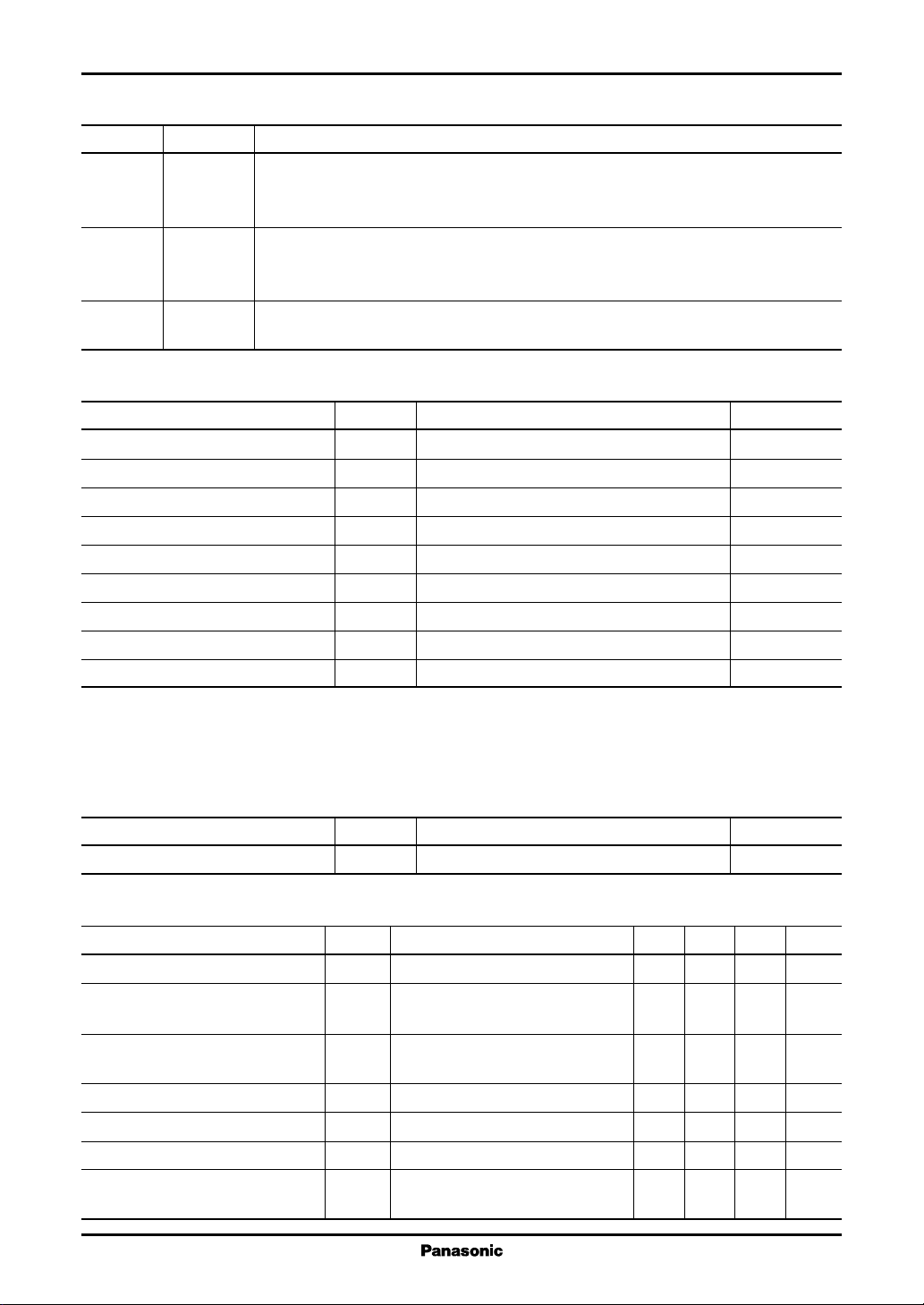
■ Block Diagram
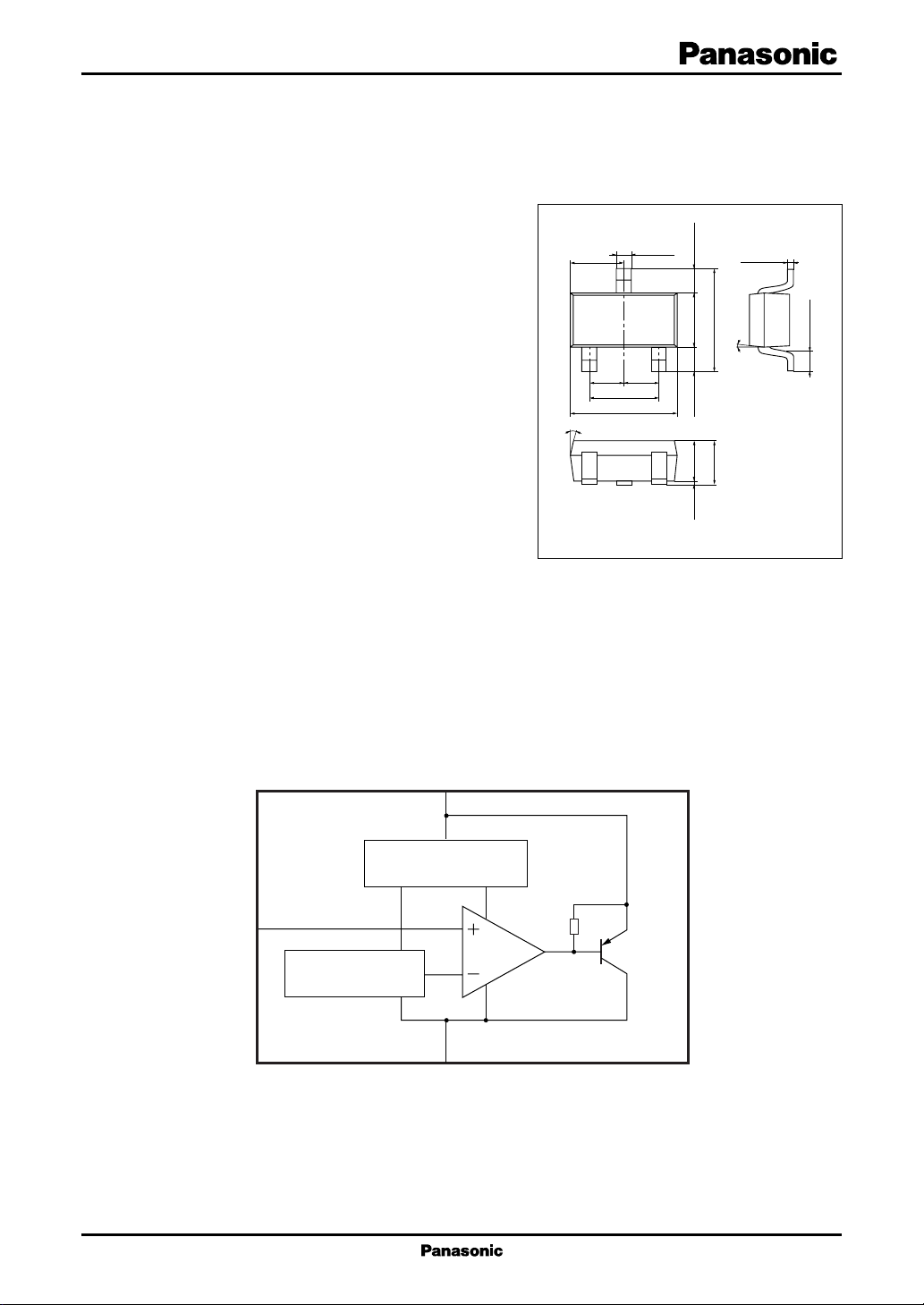
10°
1.45
1
0.95
1.90
2.90
± 0.20
+ 0.20
– 0.05
0.40
3
2
0.95
+ 0.10
– 0.05
0.65 ± 0.15
– 0.05
+ 0.25
1.50
0.65 ± 0.15
– 0.10
+ 0.20
1.10
0 to 0.1
MINI-3D
+ 0.20
2.80
– 0.30
+ 0.30
1.10
– 0.10
0.16
5°
Unit: mm
+ 0.10
– 0.06
0.40 ± 0.20
Ref.
1
Reference voltage
23
Constant current source
Error
amplifier
AK
Output
transistor
1
AN1432MS Voltage Regulators
■ Pin Descriptions
Pin No. Symbol Description
1 Reference The reference voltage (1.26 V typical) pin. Although the impedance is high under the no-
rmal using conditions, be careful that the impedance drops and current flo
inside if a current or voltage is forced to apply from the outside.
2 Cathode The pin for the combined use of the power source current supply of IC and the constant
voltage output as the shunt regulator. An excessive current supplied to this pin is bypassed
to the anode pin through the output transistor.
3 Anode The constant voltage reference pin of the shunt regulator and flows out the current from
the cathode and reference. Usually grounded.
■ Absolute Maximum Ratings
Parameter Symbol Rating Unit
Supply voltage V
Reference voltage V
Supply current I
Reference current I
Cathode anode reverse current −I
Cathode reference reverse current −I
2
Power dissipation
Operating ambient temperature
Storage temperature
Note) 1. Do not apply external currents or voltages to any pins not specifically mentioned.
For circuit currents, '+' denotes current flowing into the IC, and '−' denotes current flowing out of the IC.
1: Except for the operating ambient temperature and storage temperature, all ratings are for Ta = 25°C.
2. *
2: The value at Ta = 85°C.
*
*
1
*
1
*
T
T
REF
K
REF
KA
KR
P
opr
stg
K
D
15 V
7V
20 mA
50 µA
−10 mA
−10 mA
104 mW
−30 to +85 °C
−55 to +150 °C
ws into the IC
■ Recommended Operating Range
Parameter Symbol Range Unit
Supply voltage V
CC
■ Electrical Characteristics at Ta = 25°C
Parameter Symbol Conditions Min Typ Max Unit
Reference voltage V
Reference voltage fluctuation 1 ∆V
Reference voltage fluctuation 2 ∆V
Reference input current I
Minimum cathode current I
Off time cathode current I
Dynamic impedance Z
2
REF
REF
/∆V
KAIK
REF
/∆V
KAIK
REF
K min
K OFF
VKA = V
KA
V
to 15 V
REF
VKA = V
V
REF
, IK = 10 mA 1.235 1.26 1.285 V
REF
≤ VKA ≤ 5 V, 1.9 3.5 mV/V
= 10 mA
5 V ≤ VKA ≤ 15 V, 1.0 2.0 mV/V
= 10 mA
RI = 10 kΩ, IK = 10 mA 2.5 4.4 µA
VKA = V
REF
VKA = 15 V, V
, f ≤ 1 kHz, 0.1 0.5 Ω
REF
= 0 V 1.0 µA
REF
290 350 µA
IK = 1 mA to 10 mA
 Loading...