

Page 1
New
(6.00)
0.20±0.10
(0.48)
(1.10)
0.80 max 6.20±0.10
5.00±0.10
3-C0.50
(6.00)
6.20±0.10
(1.10)
5.00±0.10
R 0.30
SEATING PLANE
1
22
12
34
44
11
0.10
33 23
23
44
34
12
22
33
(0.48)
0.16±0.06
111
0.10
M
0.40
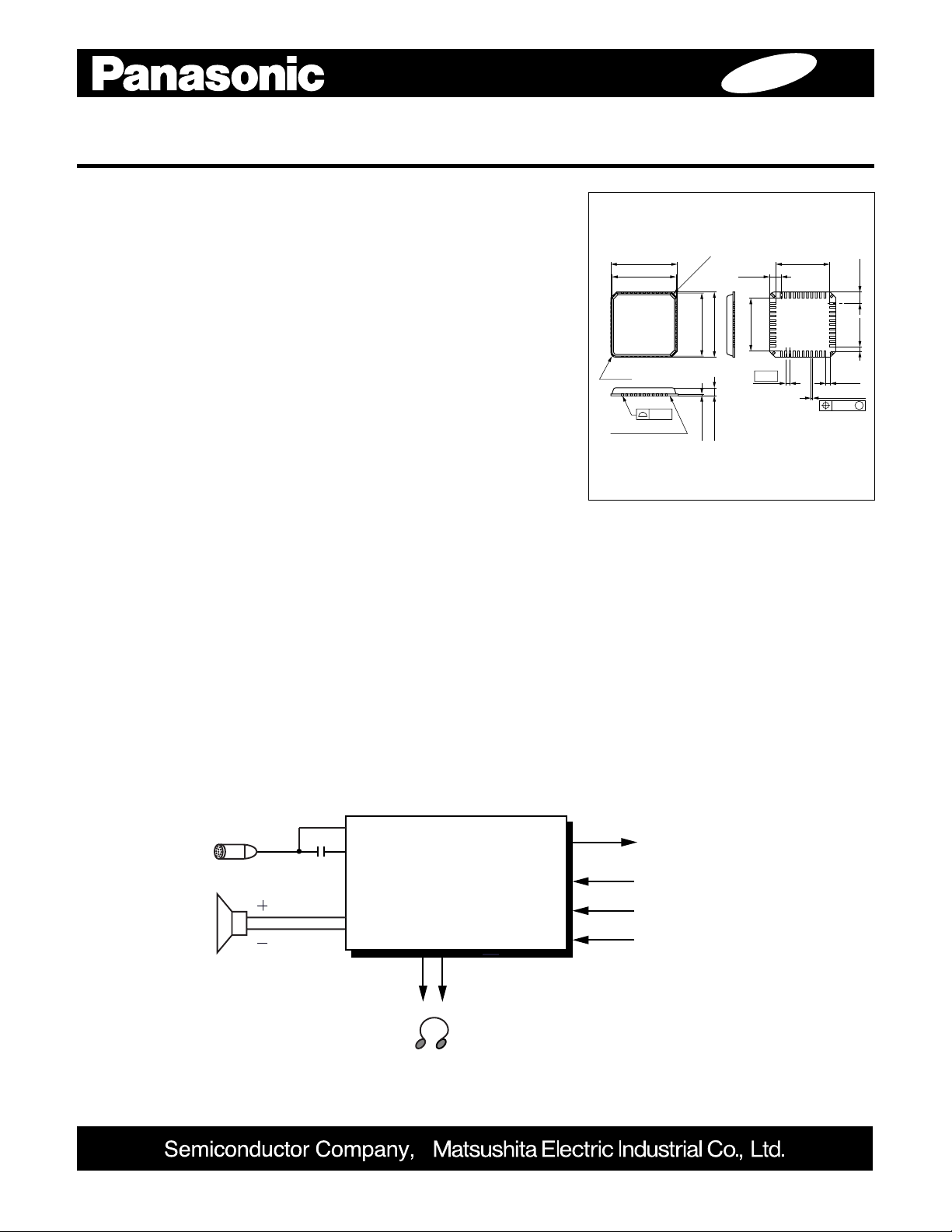
Low power drive · Mini package
Audio Interface IC AN12906A
■ Overview
The AN12906A is an input/output interface IC that has built-in audio capability.
This IC integrates in a single chip configuration a speaker amplifier , headphone
amplifier , microphone amplifier , AGC , microphone voltage supply and LPF.
Power supply voltage for Speaker-drive can drive low-voltage of 1.8 voltage.
AN12906A has the power-save function for each amplifier’s.
■ Features
● Built-in Amplifier’s.
Speaker/BTL (mono) , Headphone (stereo ) , Microphone (mono) ,LPF
● Built-in Power-save function.
Speaker-Amp. , Headphone-Amp. , Microphone-Amp. , All-Standby
● Beep-input , Input-Gain change High & Low , Mute , AGC ON/OFF
● Power supply voltage : Vcc = 2.7 V to 4.2 V , Vcc_SP = 1.8 V to 4.2 V
● Speaker absolute maximum rating : 270 mW (typ)
● Package : QFN44-pin
■ Applications
● IC-Recorder , PDA , DSC , etc.
Unit:mm
QFN044-P-0606A
■ Applications Circuit
Supply for Microphone
Audio Rec OUT
MIC IN
SP
AN12906A
HP OUT
LR
¶ The products and specifications are subject to change without any notice. Please ask for the latest product standards to guarantee the satisfaction of your product requirements.
1 Kotari-Yakemachi, Nagaokakyo, Kyoto 617-8520, Japan Tel. (075) 951-8151 http://www.panasonic.co.jp/semicon/
E00105AE
Audio IN L-ch
Audio IN R-ch
Beep IN
New publication, effective from Nov. 27. 2001.
Page 2
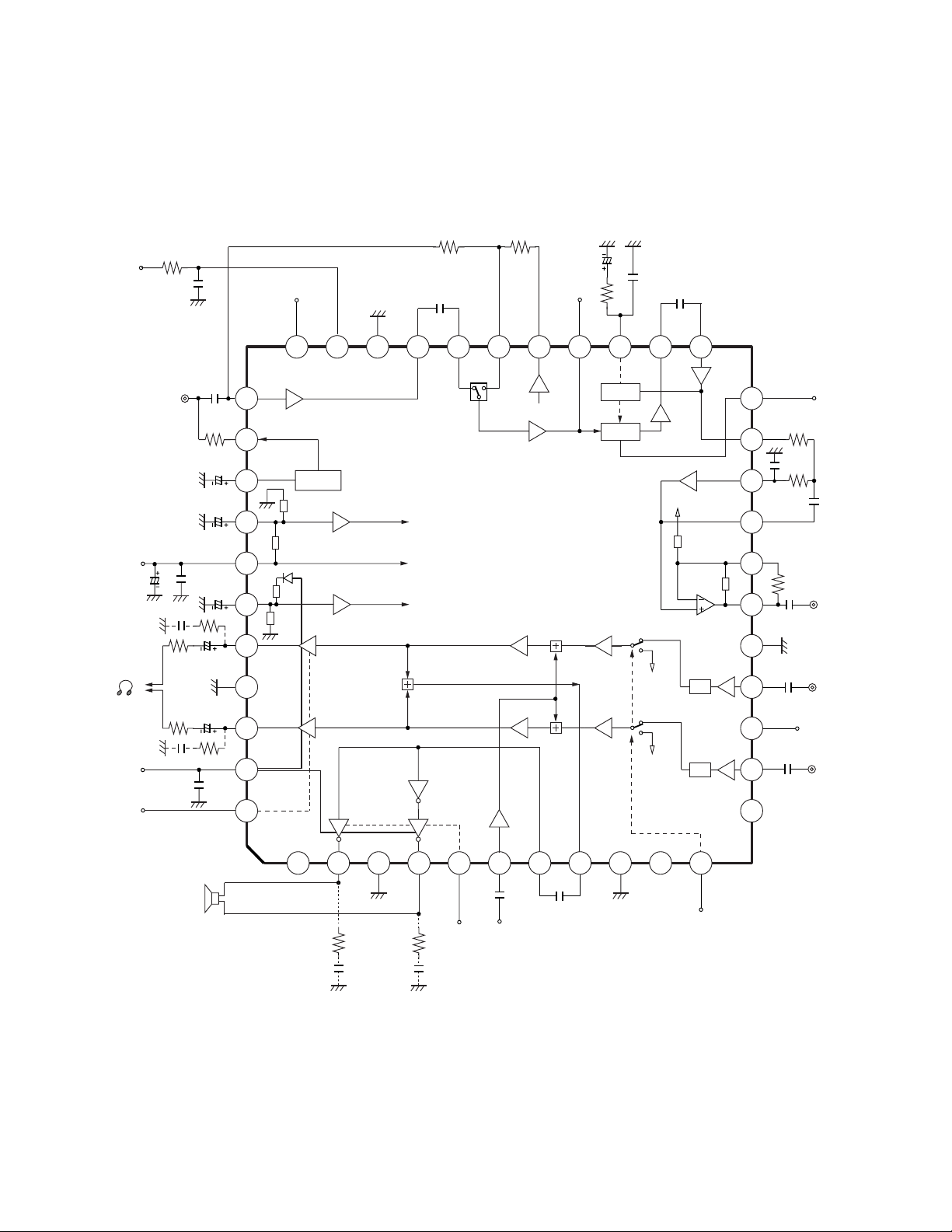
■ Block Diagram
21
20
18
17
16
14
12
33 3132 26 25 23
1110987654321
44
43
42
41
39
37
36
34
40
Mic voltage
Supply
Det
AGC
LPF
Vref
Vcc
VrefHP
LPF
15
13
2.2Ω0.1µF
2.2Ω0.1µF
0.47µF
0.47µF
0.47µF
15kΩ
18.8kΩ
2.17kΩ
0.47µF
35
1µF
10µF
38
0.01µF
10µF
0.01µF
1µF
0.1µF 2.2Ω
15Ω 220µF
15Ω 220µF
0.1µF 2.2Ω
30 29 28
22
19
0.47µF
Mute
ON/OFF
NC
Audio IN R-ch
Audio IN L-ch
STB ON/OFF
Audio Rec Out
AGC ON/OFF
220kΩ
27kΩ
0.47µF
1.0µF
0.47µF
Mic Amp
ON/OFF
Mic IN
Vcc
+3.3 V
Vcc_SP
+3.3 V
HP
GND
HP
Save
SP
GND
SP
Save
NC
HP
16Ω
SP
8Ω
+
−
Vref
L-ch
R-ch
0.47µF
Gain Change
High/Low
NC
0.47
µF
Beep IN
Vref
150pF
330pF
10kΩ
10kΩ
0.47µF
27kΩ
100kΩ
2427
Gain Change
circuit Output
Vref
(Note) • Circui,circuit constant show an example and don't guaratee design of set.
• The condenser and the resistor for the osillation measure of Headphone output, speaker output is in need
of install on the bord.
• Please you make use to 20-pin and 21-pin are short, and 19-pin is open , if you don't use a low pass filter is
made up 19-pin,20-pin and 21-pin.
Page 3
■ Pin Description
Pin No. Function Pin No. Function
1 N.C 23 OP Amp. input
2 SP output (-) 24 AGC Output
3 GND (for SP) 25 AGC demodulation pin
4 SP output (+) 26 Gain change circuit output
5 SP Power save SW 27 Gain change bias output
6 Beep input 28 Gain change Low-input
7 SP amp. input 29 Gain change High-input
8 MIX amp. output 30 MIC amp. output
9 GND 31 GND
10 N.C 32 Gain change SW
11 Mute ON/OFF SW 33 MIC amp. power save SW
12 N.C 34 MIC amp. input
13 Playback input R-ch 35 MIC supply
14 Standy SW 36 MIC supply filter
15 Playback input L-ch 37 1/2 VCC (V
16 GND 38 V
17 REC output 39 1/2 V
CC_SP
CC
(V
)
REF
REF_SP
)
18 Feedback pin for Rec-out amp. 40 HP output L-ch
19 LPF2 OP Amp. output 41 GND (for HP)
20 LPF2 OP Amp. input 42 HP output R-ch
21 OP Amp. output 43 V
(for SP drive)
CC_SP
22 AGC ON/OFF SW 44 HP power save SW
■ Absolute Maximum Ratings
Parameters
Storage temperature
Operating ambient temperature
Supply voltage
Supply current
Power dissipation
Note1) All items are at Ta = 25°C, except for the operating ambient temperature and storage temperature parameters.
The range under Absolute Maximum Ratings, Power dissipation.
Note2)
Note3)
Power dissipation shows the value of only package at Ta=70°C
Symbol
T
T
VCC/V
I
P
stg
opr
CC
D
CC_SP
Rating
-55 to +125
-20 to +70
4.5
-
194.2
Unit
°C
°C
V
mA
mW
Note
1
1
2
3
■ Recommended Operating Range
Supply voltage
V
Vcc
CC_SP
2.7 V to 4.2 V
1.8 V to 4.2 V
(Note 2)
Page 4

■ Electrical Characteristics at Ta = 25 °C ± 2 °C,VCC = 3 .0V , V
Parameters Symbol Conditions min typ max Unit
Circuit current
Circuit current without signal 1AH I
A1 V
VCC
(VCC-system, MIC Amp. ON)
Circuit current without signal 2AH I
(V
-system, MIC Amp. ON)
CC_SP
Circuit current at SP,HP save mode 1B I
A2 V
VCC
B1 Without signal 2.0 4.0 6.0 mA
VCC
(VCC-system, MIC Amp. ON) V
Circuit current at SP,HP save mode 2B I
(V
-system, MIC Amp. ON) V
CC_SP
Circuit current at standby mode 1C I
B2 Without signal − 0.1 0.5 mA
VCC
C1 Without signal − 10 20 µA
VCC
(VCC-system) V14 = 0 V
Circuit current at standby mode 2C I
C2 Without signal − 0.1 10 µA
VCC
(VCC_SP -system) V14 = 0 V
Circuit current without signal 1DH I
D1 V
VCC
(VCC-system, MIC Amp. ON)
Circuit current without signal 2DH I
(V
-system, MIC Amp. OFF)
CC_SP
Circuit current without signal 1ES I
D2 V
VCC
E1 V
VCC
(VCC-system, MIC Amp. OFF)
Circuit current without signal 2ES I
(V
-system, MIC Amp. OFF)
CC_SP
Circuit current at SP,HP save mode 1F I
E2 V
VCC
F1 Without signal 1.5 3.5 5.5 mA
VCC
(VCC-system, MIC Amp. OFF) V
Circuit current at SP,HP save mode 2F I
(V
-system, MIC Amp. OFF) V
CC_SP
Circuit current at V
open mode 1G I
CC_SP
F2 Without signal − 0.1 0.5 mA
VCC
G Without signal 2.6 4.6 6.6 mA
VCC
(VCC-system, MIC Amp. ON) V
Circuit current at V
open mode 1H I
CC_SP
H Without signal 2.0 4.0 6.0 mA
VCC
(VCC-system, MIC Amp. OFF) V
Circuit current at V
open mode 1I I
CC_SP
I Without signal − 10 20 µA
VCC
(VCC-system, Standby) V
= 3 V , V5 = 0 V 4.3 6.3 8.3 mA
33
= 3 V , V5 = 0 V 0.5 1.9 6.0 mA
33
= 3 V , V5 = 0 V , V
33
= 3 V , V5 = 0 V , V
33
= 0 V , V5 = 0 V 4.0 6.0 8.0 mA
33
= 0 V , V5 = 0 V 0.5 1.9 6.0 mA
33
= 0 V , V
33
= 0 V , V
33
= 0 V , V5 = 0 V , V
33
= 0 V , V5 = 0 V , V
33
= 3 V , V5 = 0 V , V
33
= 0 V , V5 = 0 V , V
33
= 0 V
14
= 0 V
44
= 0 V
44
= 0 V 3.0 5.0 7.0 mA
44
= 0 V 1.0 5.0 8.0 mA
44
= 0 V
44
= 0 V
44
= 0 V
44
= 0 V
44
CC_SP
= 2.5 V
Page 5

■ Electrical Characteristics at Ta = 25 °C ± 2 °C,VCC = 3 .0 V,V
CC_SP
Parameters Symbol Conditions min typ max Unit
Power supply for microphone
Microphone power supply V
MIC
Microphone amp. characteristics Microphone amp. input→ Microphone amp. output
Output level V
Output distortion TH
Output noise N
Maximum input level TH
ROM
ROM1Vin
ROM
ROM2
Rec. AGC characteristics AGC input→Rec. output REF = -50 dBS
Rec. output level A V
ROA
( REF -3dB )
Rec. output distortion 1A TH
ROA
( REF -3dB )
Rec. output noise voltage A VN
Microphone AGC characteristics 1 V
ROA
AGCML1
(REF +3 dB)
Microphone AGC characteristics 2 V
AGCML2
(REF +20dB)
Microphone AGC characteristics 3 V
AGCML3
(REF +30 dB)
Microphone AGC characteristics 4 V
AGCM4
(REF +40 dB)
Microphone AGC characteristics 4 TH
AGCM4
distortion(REF +40 dB) up to 5 th THD,load = 22 kΩ
HP output characteristics at playback PB input→HP output
HP Reference output level V
HP Reference output distortion TH
HP Reference output noise VN
HP Maximum output level V
Output noise at HP mute mode V
PB maximum output level V
Output level at power save mode V
Beep output level V
LOPS
LOPS
OPS
LMAPOS
LMUPOS
LMAPIS
PHPPS
HPBEP
with output current -5 mA 1.8 2.0 2.2 V
Vin = -37 dBS,1 kHz -21 -20 -19 dBS
= -37 dBS,1 kHz,up to 5 th THD − 0.02 0.10 %
Without input signal,using A-curve filter − -101 -97 dBS
Vin = -27 dBS,1 kHz,up to 5 th THD,load = 22 kΩ
Vin = -53 dBS,1 kHz -16.3 -15.3 -14.3 dBS
Vin = -53 dBS,1 kHz,up to 5 th THD − 0.02 0.10 %
With out input signal,using A-curve filter − -71 -67 dBS
Vin = -47 dBS,1 kHz -14 -12 -10 dBS
Vin = -30 dBS,1 kHz -14 -11 -8 dBS
Vin = -20 dBS,1 kHz -14 -11 -8 dBS
Vin = -10 dBS,1 kHz -12.5 -9.5 -6.5 dBS
Vin = -10 dBS,1 kHz − 0.2 1.0 %
Vin = -28.3 dBS,1 kHz,load = 31 Ω -18.3 -16.3 -14.3 dBS
Vin = -28.3 dBS,1 kHz,up to 5 th THD − 0.10 0.50 %
load = 31 Ω
Without input signal,using A-curve filter − -87 -82 dBS
load = 31 Ω
f = 1 kHz,load = 31 Ω -3.5 -1.5 − dBS
input level THD = 1 % (up to 5 th)
Without input signal,using A-curve filter − -89 -84 dBS
load = 31 Ω,V11=0 V
f = 1 kHz,load = 31 Ω -15.5 -13.5 − dBS
input level THD = 1 % (up to 5 th)
Vin = -28.3 dBS,1 kHz, − -111 -110 dBS
Using A-curve filter,load = 31 Ω
Vin=2.7 dBS,1 kHz,load = 31 Ω -18.3 -16.3 -14.3 dBS
= 2.5 V
− 0.02 1.0 %
Page 6

■ Electrical Characteristics at Ta = 25 °C ± 2 °C,VCC = 3 .0 V,V
Parameters Symbol Conditions min typ max Unit
SP output characteristics
SP reference output level V
SPPS
at playback load = 8 Ω,
SP reference output distortion TH
SPPS
at playback load = 8 Ω,up to 5 th THD
SP reference output noise VN
SPPS
at playback load = 8Ω
SP output noise at mute and V
SMUPOS
playback V11=0 V,load = 8Ω
SP maximum rating output V
MSPPS
at playback
SP output V
PSPPS
at power save and playback Using A-curve filter,load = 8 Ω
SP: beep output level V
SPBEP
at playback load= 8 Ω
Mode selection hold voltage
MIC amp. off hold voltage range V
MIC amp. on hold voltage range V
MIC amp. ON/OFF pin open voltage V
Gain low hold voltage range V
Gain high hold voltage range V
AGC off hold voltage range V
AGC on hold voltage range V
Standby on hold voltage range V
Standby off hold voltage range V
SP output off hold voltage range V
SP output on hold voltage range V
HP output off hold voltage range V
HP output on hold voltage range V
Mute on hold voltage range V
Mute off hold voltage range V
33L
33H
33MIC
32L
32H
22L
22H
14L
14H
5L
5H
44L
44H
11L
11H
Vin = -28.3 dBS,1 kHz -3.3 -1.3 +0.7 dBS
Vin = -28.3 dBS,1 kHz − 0.2 0.9 %
Without input signal,using A-curve filter − -76 -71 dBS
Without input signal,using A-curve filter − -78 -73 dBS
f = 1 kHz 200 270 − mW
R
= 8 Ω,THD = 10 %
OUT
Vin = -28.3 dBS,1 kHz − -111 -100 dBS
Vin = -2.7 dBS,1 kHz -3.3 -1.3 +0.7 dBS
− 0 − 0.5 V
− 2.5 − 3.0 V
V
= 3.0 V , 33-pin open 0.0 0.05 0.5 V
CC
− 0 − 0.5 V
− 2.5 − 3.0 V
− 0 − 0.5 V
− 2.5 − 3.0 V
− 0 − 0.5 V
− 2.5 − 3.0 V
− 0 − 0.5 V
− 2.5 − 3.0 V
− 0 − 0.5 V
− 2.5 − 3.0 V
− 0 − 0.5 V
− 2.5 − 3.0 V
CC_SP
= 2.5 V
Page 7

■ Package Power Dissipation
1400
1392
1200
1000
(mW)
D
800
600
In standard board (Grass epoxy:50×50×0.8mm3)
Rth(j-a)=71.8 °C/W
Power Dissipation P
400
353
200
Rth(j-a)=282.9 °C/W
0
0
Package only
25 50 75 100
Ambient Temperature Ta (°C)
125
Page 8

Request for your special attention and precautions in using the technical information
and semiconductors described in this material
(1) An export permit needs to be obtained from the competent authorities of the Japanese Govern-
ment if any of the products or technologies described in this material and controlled under the
"Foreign Exchange and Foreign Trade Law" is to be exported or taken out of Japan.
(2) The technical information described in this material is limited to showing representative character-
istics and applied circuit examples of the products. It does not constitute the warranting of industrial
property, the granting of relative rights, or the granting of any license.
(3) The products described in this material are intended to be used for standard applications or gen-
eral electronic equipment (such as office equipment, communications equipment, measuring instruments and household appliances).
Consult our sales staff in advance for information on the following applications:
· Special applications (such as for airplanes, aerospace, automobiles, traffic control equipment,
combustion equipment, life support systems and safety devices) in which exceptional quality and
reliability are required, or if the failure or malfunction of the products may directly jeopardize life or
harm the human body.
· Any applications other than the standard applications intended.
(4) The products and product specifications described in this material are subject to change without
notice for reasons of modification and/or improvement. At the final stage of your design, purchasing, or use of the products, therefore, ask for the most up-to-date Product Standards in advance to
make sure that the latest specifications satisfy your requirements.
(5) When designing your equipment, comply with the guaranteed values, in particular those of maxi-
mum rating, the range of operating power supply voltage and heat radiation characteristics. Otherwise, we will not be liable for any defect which may arise later in your equipment.
Even when the products are used within the guaranteed values, redundant design is recommended,
so that such equipment may not violate relevant laws or regulations because of the function of our
products.
(6) When using products for which dry packing is required, observe the conditions (including shelf life
and after-unpacking standby time) agreed upon when specification sheets are individually exchanged.
(7) No part of this material may be reprinted or reproduced by any means without written permission
from our company.
Please read the following notes before using the datasheets
A. These materials are intended as a reference to assist customers with the selection of Panasonic
semiconductor products best suited to their applications.
Due to modification or other reasons, any information contained in this material, such as available
product types, technical data, and so on, is subject to change without notice.
Customers are advised to contact our semiconductor sales office and obtain the latest information
before starting precise technical research and/or purchasing activities.
B. Panasonic is endeavoring to continually improve the quality and reliability of these materials but
there is always the possibility that further rectifications will be required in the future. Therefore,
Panasonic will not assume any liability for any damages arising from any errors etc. that may appear in this material.
C. These materials are solely intended for a customer's individual use.
Therefore, without the prior written approval of Panasonic, any other use such as reproducing,
selling, or distributing this material to a third party, via the Internet or in any other way, is prohibited.
2001 MAR
 Loading...