

Panasonic 2SK3193 User Manual
Power MOSFETs
This product complies with the RoHS Directive (EU 2002/95/EC).
2SK3193
Silicon N-channel power MOSFET
For switching
■ Features
• Avalanche energy capability guaranteed
• High-speed switching
• Low ON resistance R
• No secondary breakdown
■ Absolute Maximum Ratings TC = 25°C
Parameter Symbol Rating Unit
Drain-source surrender voltage V
Gate-source surrender voltage V
Drain current I
Peak drain current I
Avalanche energy capability
Power dissipation P
Channel temperature T
Storage temperature T
Note)*:L = 1 mH, IL = 20 A, 1 pulse, Ta = 25°C
on
DSS
GSS
D
DP
*
EAS 200 mJ
D
350 V
±30 V
±20 A
±80 A
100 W
Ta = 25°C3
ch
stg
150 °C
−55 to +150 °C
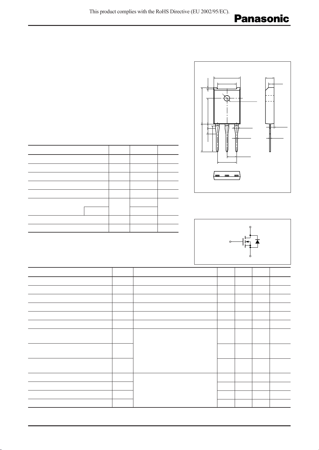
15.0±0.3
11.0±0.2
(0.7)
φ 3.2±0.1
±0.2
21.0±0.516.2±0.5
15.0
(2.3)
(3.2)
Solder Dip
10.9±0.5
123
2.0±0.2
1.1±0.1
5.45±0.3
Marking Symbol: K3193
Internal Connection
G
Unit: mm
5.0±0.2
(3.2)
2.0±0.1
0.6±0.2
1: Gate
2: Drain
3: Source
EIAJ: SC-92
TOP-3F-B1 Package
D
■ Electrical Characteristics TC = 25°C ± 3°C
S
Parameter Symbol Conditions Min Typ Max Unit
Drain-source surrender voltage V
Drain-source cutoff current I
Gate-source cutoff current I
Gate threshold voltage V
Drain-source ON resistance R
DSSID
DSS
GSS
DS(on)VGS
= 1 mA, VGS = 0 350 V
VDS = 280 V, VGS = 010µA
VGS = ±30 V, VDS = 0 ±1 µA
VDS = 10 V, ID = 1 mA 2 4 V
th
= 10 V, ID = 10 A 120 150 mΩ
Forward transfer admittance Yfs VDS = 10 V, ID = 10 A 6 12 S
Short-circuit forward transfer capacitance C
VDS = 10 V, VGS = 0, f = 1 MHz 3 900 pF
iss
(Common source)
Short-circuit output capacitance C
oss
1 340 pF
(Common source)
Reverse transfer capacitance C
rss
560 pF
(Common source)
Turn-on delay time t
Rise time t
Turn-off delay time t
Fall time t
Publication date: November 2004 SJG00039AED
VDD = 150 V, ID = 10 A 40 ns
d(on)
RL = 15 Ω, VGS = 10 V 75 ns
r
d(off)
f
340 ns
95 ns
1
2SK3193
This product complies with the RoHS Directive (EU 2002/95/EC).
■ Electrical Characteristics (continued) TC = 25°C ± 3°C
Parameter Symbol Conditions Min Typ Max Unit
Diode forward voltage V
Reverse recovery time t
Reverse recovery charge Q
Gate charge load Q
Gate-source charge Q
Gate-drain charge Q
Thermal resistance (ch-c) R
Thermal resistance (ch-a) R
DSFIDR
rr
rr
g
gs
gd
th(ch-c)
th(ch-a)
Note) Measuring methods are based on JAPANESE INDUSTRIAL STANDARD JIS C 7030 measuring methods for transistors.
= 20 A, VGS = 0 −1.4 V
L = 230 µH, VDD = 100 V 260 ns
IDR = 10 A, di/dt = 100 A/µs 1.8 µC
VDD = 100 V, ID = 10 A 90 nC
VGS = 10 V 10 nC
30 nC
1.25 °C/W
41.7 °C/W
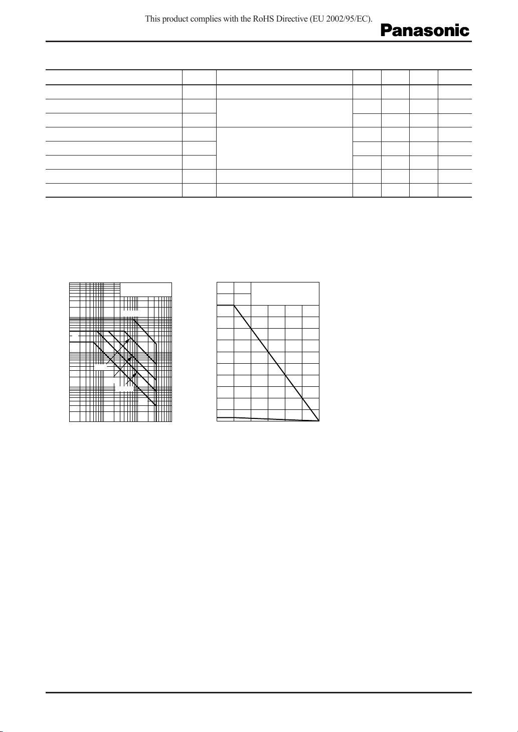
Safe operation area PD T
3
10
I
DP
2
10
)
A
(
D
I
D
10
Drain current I
1
−1
10
11010210
Drain-source voltage VDS (V
1 ms
10 ms
Non repetitive pulse
TC = 25°C
t = 100 µs
100 ms
DC
120
(1)
100
)
W
(
80
D
60
40
a
(1) TC = T
a
(2) Without heat sink
= 3 W
P
D
Power dissipation P
20
(2)
3
)
0
0 50 150100
Ambient temperature Ta (°C
)
2
SJG00039AED
 Loading...