

Panasonic 2SK2538 Datasheet
Power F-MOS FETs 2SK2538
2SK2538
Silicon N-Channel Power F-MOS
■ Features
●
Avalanche energy capability guaranteed
●
High-speed switching
●
No secondary breakdown
■ Applications
●
High-speed switching (switching mode regulator)
●
For high-frequency power amplification
■ Absolute Maximum Ratings (Tc = 25˚C)
Parameter
Drain-Source breakdown voltage
Gate-Source voltage
Drain current
DC
Pulse
Avalanche energy capability
= 25˚C
T
Allowable power
dissipation
C
Ta= 25˚C
Channel temperature
Storage temperature
* L= 5mH, IL= 2A, VDD= 30V, 1 pulse
Symbol
V
DSS
V
GSS
I
D
I
DP
*
EAS
P
D
T
ch
T
stg
Rating
250
±30
±2
±4
10
30
2
150
–55 to +150
Unit
V
V
A
A
mJ
W
˚C
˚C
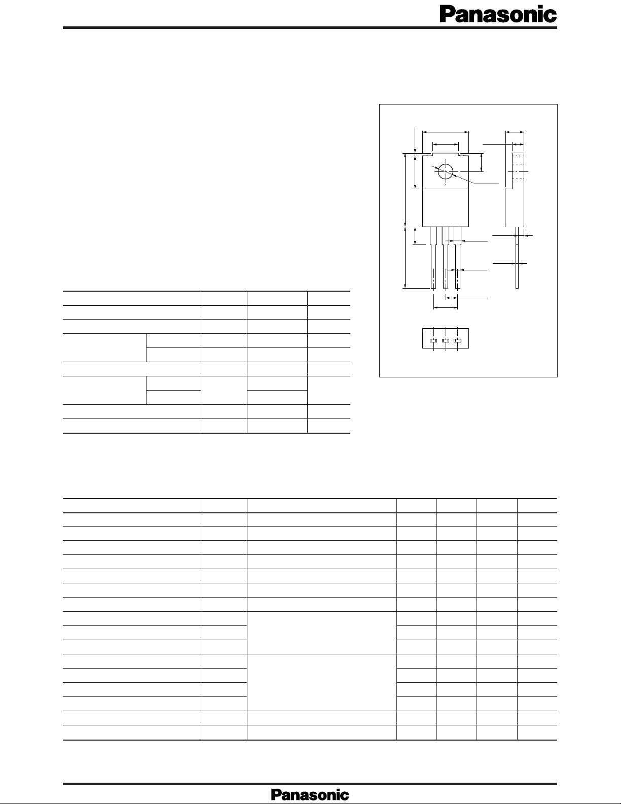
16.7±0.3
14.0±0.5
0.7±0.1
7.5±0.2
4.0
Solder Dip
10.0±0.2
5.5±0.2
5.08±0.5
213
2.7±0.2
4.2±0.2
ø3.1±0.1
1.3±0.2
1.4±0.1
+0.2
0.5
0.8±0.1
2.54±0.25
TO-220 Full Pack Package (a)
-
Unit : mm
4.2±0.2
0.1
1 : Gate
2 : Drain
3 : Source
■ Electrical Characteristics (Tc = 25˚C)
Parameter
Drain-Source cut-off current
Gate-Source leakage current
Drain-Source breakdown voltage
Gate threshold voltage
Drain-Source ON-resistance
Forward transadmittance
Diode forward voltage
Input capacitance
Output capacitance
Feedback capacitance
Turn-on time (delay time)
Rise time
Fall time
Turn-off time (delay time)
Channel-Case heat resistance
Channel-Atmosphere heat resistance
Symbol
I
DSS
I
GSS
V
DSS
V
th
R
DS(on)
| Yfs |
V
DSF
C
iss
C
oss
C
rss
t
d(on)
t
r
t
f
t
d(off)
R
th(ch-c)
R
th(ch-a)
V
V
I
D
V
V
V
I
DR
V
V
V
Condition
= 200V, VGS= 0
DS
=±30V , VDS= 0
GS
=1mA, VGS= 0
=10V, ID=1mA
DS
=10V, ID=1A
GS
= 25V, ID=1A
DS
= 2A, VGS= 0
=10V , VGS= 0, f=1MHz
DS
= 200V, ID= 2A
DD
=10V, RL=100Ω
GS
Min
250
1
0.5
Typ
1.2
1
220
60
20
10
20
45
90
Max
100
±1
5
2
–1.6
4.17
62.5
Unit
µ A
µ A
V
V
Ω
S
V
pF
pF
pF
ns
ns
ns
ns
˚C/W
˚C/W
Power F-MOS FETs 2SK2538
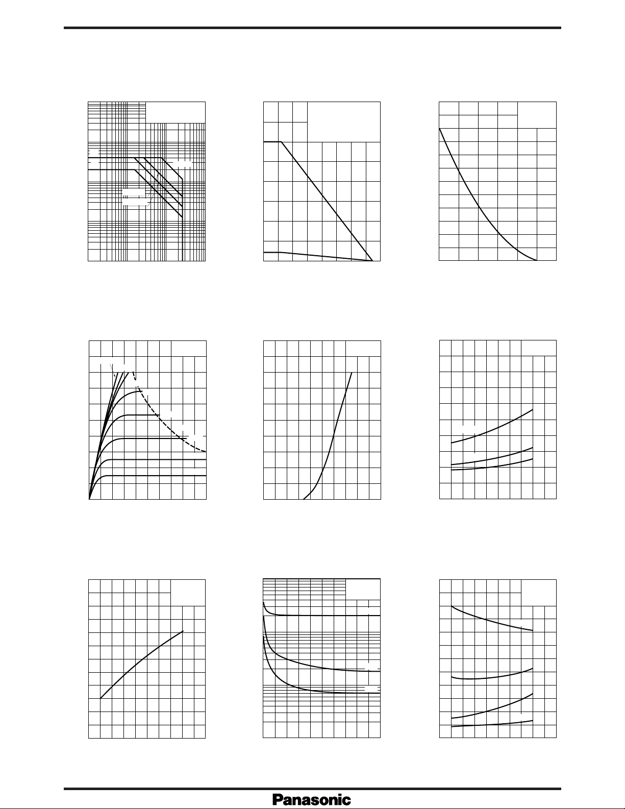
Area of safe operation (ASO)
100
30
10
)
I
DP
A
(
3
I
D
D
1
0.3
Drain current I
0.1
0.03
0.01
1
Drain-Source voltage V
5
VGS=10.0V
4
)
A
(
D
3
2
Drain current I
1
Non repetitive pulse
T
=25˚C
C
t=1ms
t=10ms
t=100ms
DC
10 100 10003 30 300
DS
ID – V
DS
9.0V
8.0V
7.0V
6.5V
30W
(V)
TC=25˚C
6.0V
5.5V
5.0V
PD – T a
40
(1) TC=Ta
)
W
(
(1)
30
D
20
10
Allowable power dissipation P
(2)
0
0
Ambient temperature Ta (˚C
(2) Without heat sink
(P
40 80 120 16020 60 100 140
ID – V
5
4
)
A
(
D
3
2
Drain current I
1
=2.0W)
D
GS
)
VDS=10V
T
=25˚C
C
EAS – T
12
10
8
6
4
2
Avalanche energy capability EAS (mJ)
0
25 50
5
)
Ω
(
4
DS(on)
3
2
1
Drain-Source ON-resistance R
75 100 125 150 175
Junction temperature T
R
DS(on)
TC=100˚C
25˚C
0˚C
– I
j
VDD=30V
I
D
j
D
V
=2A
(˚C)
GS
=10V
0
048121620
D
DS
D
(V
VDS=25V
T
(A)
)
=25˚C
C
Drain voltage V
| Yfs | – I
3
)
S
(
|
fs
2
1
Forward transadmittance | Y
0
012345
Drain current I
0
0246810
Gate-Source voltage V
C
iss, Coss, Crss
)
1000
F
(p
rss
, C
300
oss
, C
iss
C
100
30
Feedback capacitance
10
3
Input capacitance, Output capacitance,
1
0 50 100 150 200 250
Drain-Source voltage V
– V
GS
f=1MHz
T
DS
(V)
DS
=25˚C
C
(V)
0
012345
Drain current I
t
d(on), tr, tf, td(off)
120
C
iss
C
oss
C
rss
100
)
ns
80
(
60
40
Switching time t
20
0
012345
Drain current ID (A
D
t
t
t
t
(on)
d
(A)
–
I
D
VDD=200V
V
=10V
GS
T
=25˚C
C
(off)
d
f
r
)
 Loading...