

Panasonic 2SK2380 Datasheet
Silicon Junction FETs (Small Signal)
2SK2380
Silicon N-Channel Junction FET
For impedance conversion in low frequency
For infrared sensor
■ Features
●Low gate to source leakage current, I
●Small capacitance of C
, C
iss
oss
●SS-mini type package, allowing downsizing of the sets and auto-
matic insertion through the tape/magazine packing.
, C
GSS
rss
■ Absolute Maximum Ratings (Ta = 25°C)
Parameter
Gate to Drain voltage
Gate to Source voltage
Drain current
Gate current
Allowable power dissipation
Channel temperature
Storage temperature
Symbol
V
GDO
V
GSO
I
D
I
G
P
D
T
ch
T
stg
Ratings
−40
−40
±1
10
125
125
−55 to +125
Unit
V
V
mA
mA
mW
°C
°C
■ Electrical Characteristics (Ta = 25°C)
Parameter
Drain to Source cut-off current
Gate to Source leakage current
Gate to Drain voltage
Gate to Source cut-off voltage
Forward transfer admittance
Input capacitance (Common Source)
Output capacitance (Common Source)
Reverse transfer capacitance (Common Source)
Symbol
*
I
DSS
I
GSS
V
DS
V
GSC
| Yfs |
C
iss
C
oss
C
rss
VDS = 10V, VGS = 0
VGS = −20V, VDS = 0
IG = −10µA, VDS = 0
VDS = 10V, ID = 1µA
VDS = 10V, VGS = 0, f = 1kHz
VDS = 10V, VGS = 0, f = 1MHz
Conditions
1.6±0.15
0.8±0.1 0.40.4
1
0.5
1.6±0.1
1.0±0.1
0.5
2
0.3
0.75±0.15
0.45±0.1
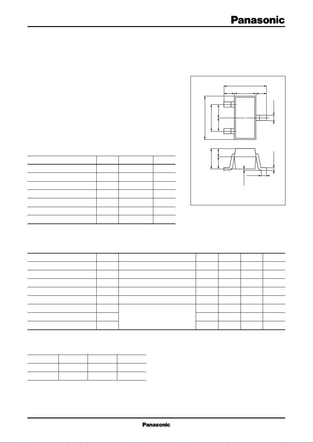
1: Source
2: Drain EIAJ: SC-75
3: Gate SS-Mini Type Package (3-pin)
0.2±0.1
0 to 0.1
unit: mm
+0.1
3
+0.1
Marking Symbol (Example): EB
min
50
−40
0.05
typ
−1.3
1
0.4
0.4
max
200
− 0.5
−3
Unit
µA
nA
mS
pF
pF
pF
–0.05
0.2
–0.05
0.15
V
V
*
I
rank classification
DSS
Runk
I
(mA)
DSS
Marking Symbol
Q
50 to 100
EBQ
R
70 to 130
EBR
S
100 to 200
EBS
1
Silicon Junction FETs (Small Signal)
2SK2380
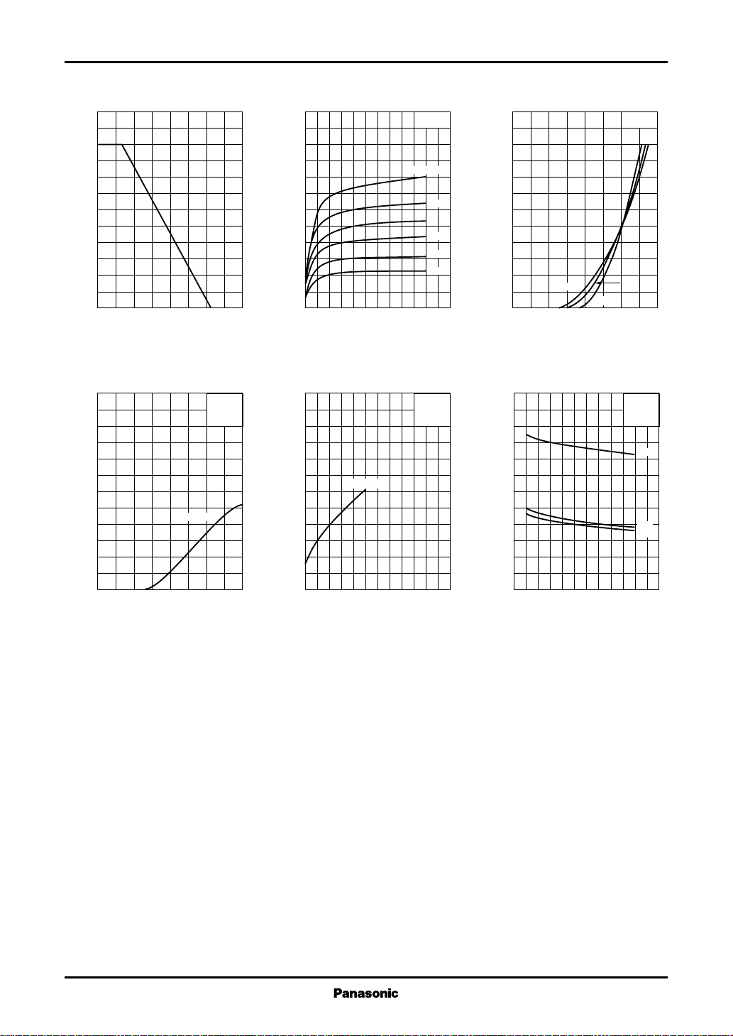
PD Ta ID V
150
)
mW
(
125
D
100
75
50
25
Allowable power dissipation P
0
0 16040 12080 14020 10060
Ambient temperature Ta (˚C
| Yfs | V
1.2
)
mS
(
1.0
|
fs
0.8
0.6
0.4
0.2
Forward transfer admittance |Y
0
–1.2 0.4– 0.8 0– 0.4
Gate to source voltage VGS (V
I
DSS
GS
=100µA
VDS=10V
f=1kHz
Ta=25˚C
DS
240
200
)
µA
(
160
D
120
80
Drain current I
40
0
012108264
)
Drain to source voltage VDS (V
| Yfs | I
240
)
mS
(
200
|
fs
160
I
=100µA
120
80
40
Forward transfer admittance |Y
0
0 24020016040 12080
)
DSS
Drain current ID (µA
Ta=25˚C
V
=0.4V
GS
0.2V
0V
– 0.2V
– 0.4V
– 0.6V
)
D
V
=10V
DS
Ta=25˚C
)
240
200
)
µA
(
160
D
120
80
Drain current I
40
0
–1.2 0.4– 0.8 0– 0.4
Gate to source voltage VGS (V
1.2
)
,
)
pF
(
1.0
rss
,C
Common source
(
oss
,C
0.8
iss
C
)
0.6
, Output capacitance
)
Common source
(
0.4
Common source
(
0.2
Input capacitance
Reverse transfer capacitance
0
012108264
Drain to source voltage VDS (V
ID V
GS
VDS=10V
Ta=75˚C
25˚C
–25˚C
)
C
, C
, C
oss
rss
V
DS
VGS=0V
Ta=25˚C
f=1MHz
C
iss
C
rss
C
oss
iss
)
2
 Loading...