

Panasonic 2SK2375 Datasheet
Power F-MOS FETs
2SK2375
Silicon N-Channel Power F-MOS FET
■ Features
●Avalanche energy capacity guaranteed
●High-speed switching
●Low ON-resistance
●No secondary breakdown
■ Applications
●Contactless relay
●Diving circuit for a solenoid
●Driving circuit for a motor
●Control equipment
●Switching power supply
■ Absolute Maximum Ratings (T
Parameter
Drain to Source breakdown voltage
Gate to Source voltage
Drain current
DC
Pulse
Avalanche energy capacity
Allowable power
dissipation
TC = 25°C
Ta = 25°C
Channel temperature
Storage temperature
*
L = 1.9mH, IL = 8A, 1 pulse
Symbol
V
V
I
D
I
DP
EAS
P
D
T
ch
T
stg
DSS
GSS
*
= 25°C)
C
Ratings
−55 to +150
900
±30
±8
±16
60
100
3
150
Unit
V
V
A
A
mJ
W
°C
°C
4.5
4.0
2.0±0.2
1.1±0.1
5.45±0.3
0.7±0.1
3.3±0.3
15.5±0.5
5˚
123
φ3.2±0.1
2.0 2.0 1.2 10.0
5.45±0.3
2.0
26.5±0.5
18.6±0.5
5.5±0.3
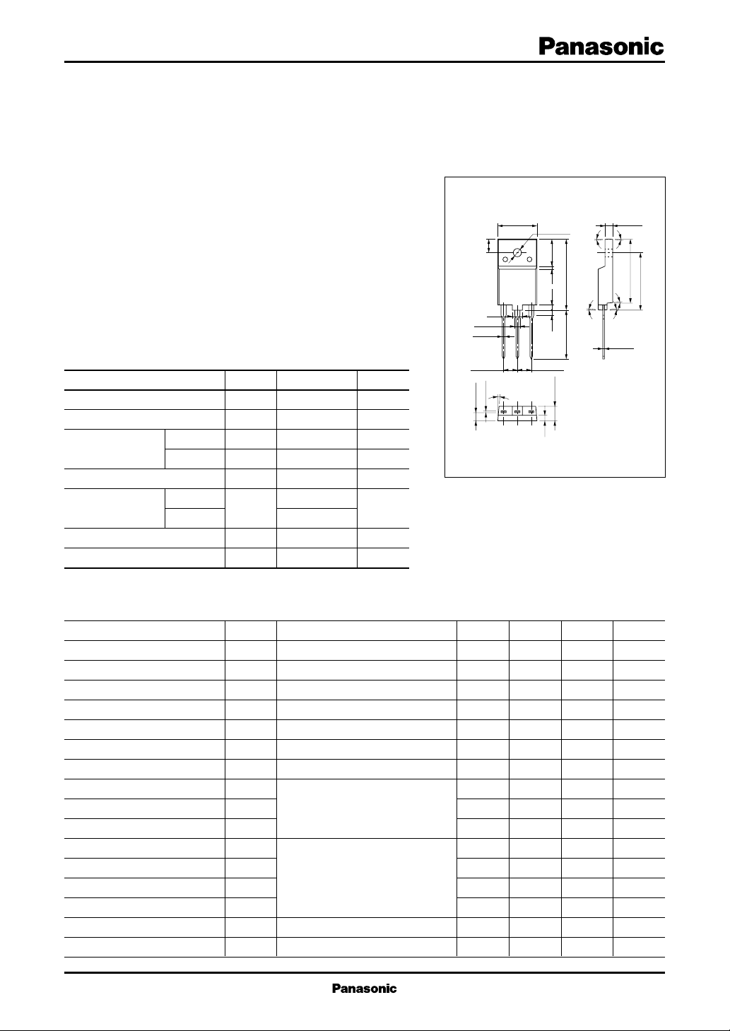
unit: mm
3.0±0.3
5˚ 5˚
23.4
5˚
5˚
5˚
0.7±0.1
1: Gate
2: Drain
3: Source
TOP-3E Package
22.0±0.5
■ Electrical Characteristics (T
Parameter
Drain to Source cut-off current
Gate to Source leakage current
Drain to Source breakdown voltage
Gate threshold voltage
Drain to Source ON-resistance
Forward transfer admittance
Diode forward voltage
Input capacitance (Common Source)
Output capacitance (Common Source)
Reverse transfer capacitance (Common Source)
Turn-on time (delay time)
Rise time
Fall time
Turn-off time (delay time)
Thermal resistance between channel and case
Thermal resistance between channel and atmosphere
C
Symbol
I
DSS
I
GSS
V
DSS
V
th
R
DS(on)
| Yfs |
V
DSF
C
iss
C
oss
C
rss
t
d(on)
t
r
t
f
t
d(off)
R
th(ch-c)
R
th(ch-a)
= 25°C)
Conditions
VDS = 720V, VGS = 0
VGS = ±30V, VDS = 0
ID = 1mA, VGS = 0
VDS = 25V, ID = 1mA
VGS = 10V, ID = 4A
VDS = 25V, ID = 4A
IDR = 8A, VGS = 0
VDS = 20V, VGS = 0, f = 1MHz
VDD = 200V, ID = 4A
VGS = 10V, RL = 50Ω
min
900
2
3
typ
1.3
5.5
1800
200
90
30
70
80
250
max
100
±1
5
1.7
−1.6
1.25
41.67
Unit
µA
µA
V
V
Ω
S
V
pF
pF
pF
ns
ns
ns
ns
°C/W
°C/W
1
Power F-MOS FETs 2SK2375
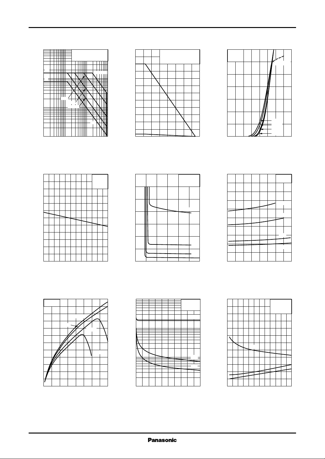
Area of safe operation (ASO) PD Ta ID V
100
30
I
DP
)
A
(
I
10
D
D
3
1
Non repetitive pulse
T
1ms
10ms
100ms
=25˚C
C
Drain current I
0.3
0.1
1 10 100 10003 30 300
Drain to source voltage VDS (V
Vth T
6
)
5
V
(
th
4
3
2
1
Gate threshold voltage V
0
0 25 50 75 100 125 150
C
Case temperature TC (˚C
t=100µs
DC
VDS=25V
=1mA
I
D
120
)
W
(
100
D
80
60
40
20
Allowable power dissipation P
0
020
)
)
Ambient temperature Ta (˚C
70
)
60
V
(
DS
50
40
30
20
10
Drain to source voltage V
0
0 5 10 15 20 25 30
Gate to source voltage VGS (V
(1) TC=Ta
(2) Without heat sink
=3W)
(P
D
(1)
(2)
40 60 80 100 120 140 160
)
VDS V
GS
TC=25˚C
=16A
I
D
8A
4A
2A
)
7
=25V
V
DS
6
)
5
A
(
D
4
3
2
Drain current I
1
0
082647153
Gate to source voltage VGS (V
5
)
Ω
(
4
DS(on)
3
2
1
Drain to source ON-resistance R
0
082647153
Drain current ID (A
R
DS(on)
GS
I
TC=150˚C
150˚C
100˚C
25˚C
0˚C
D
TC=150˚C
V
GS
100˚C
25˚C
0˚C
)
)
=10V
| Yfs | I
6
VDS=25V
)
S
(
5
|
fs
4
3
2
1
TC=0˚C
25˚C
Forward transfer admittance |Y
0
24681357
0
Drain current ID (A
2
D
100˚C
150˚C
)
C
, C
, C
iss
oss
rss
10000
)
,
)
pF
(
rss
3000
,C
Common source
(
oss
,C
1000
iss
C
)
300
, Output capacitance
)
Common source
(
100
Common source
(
30
Input capacitance
Reverse transfer capacitance
10
0 2001601208040
Drain to source voltage VDS (V
V
DS
f=1MHz
=25˚C
T
C
ton, tf, t
600
)
C
iss
C
oss
C
rss
)
500
ns
(
400
d(off)
,t
f
,t
on
300
200
100
Switching time t
0
012108264
Drain current ID (A
I
d(off)
t
d(off)
D
VDD=200V
V
=10V
GS
=25˚C
T
C
t
on
t
f
)
 Loading...