

Panasonic 2SK2211 Datasheet
Silicon MOS FETs (Small Signal)
D
S
G
2SK2211
Silicon N-Channel MOS FET
For switching
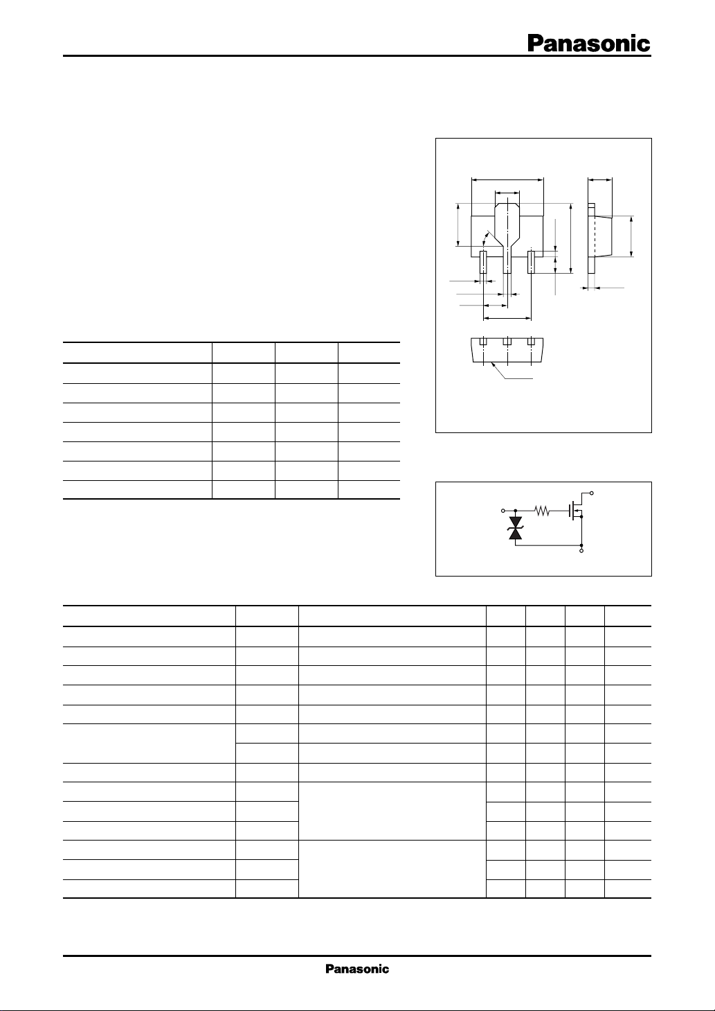
Unit : mm
1.5
4.5
±0.1
1.6
±0.2
±0.1
■ Features
• Low ON-resistance R
DS(ON)
±0.1
2.6
45˚
+0.25
0.4 max.
4.0
–0.20
• High-speed switching
0.4
• Mini-power type package, allowing downsizing of the sets and
automatic insertion through the tape/magazine packing.
■ Absolute Maximum Ratings Ta = 25°C
±0.08
0.5
±0.08
1.5
±0.1
321
–0.2
+0.1
1.0
3.0
±0.15
0.4
Parameter Symbol Ratings Unit
Drain to Source voltage V
Gate to Source voltage V
Drain current I
Max drain current I
Allowable power dissipation
*
Channel temperature P
Storage temperature T
DS
GSO
D
PD
P
D
ch
−55 to +150 °C
stg
30 V
±20 V
±1A
±2A
1W
150 °C
Marking Symbol: 2M
Internal Connection
marking
1: Gate
2: Drain
3: Source
Mini-Power Type Package (3-pin)
Note) * PC board: Copper foil of the drain portion should have a area of
1 cm2 or more and the board thickness should be 1.7 mm.
■ Electrical Characteristics Ta = 25°C
Parameter Symbol Conditions Min Typ Max Unit
Drain to Source cut-off current I
Gate to Source leakage current I
Drain to Source breakdown voltage V
Gate to Source voltage V
Gate threshold voltage V
Drain to Source ON-resistance
*
R
DS(ON)1
R
DS(ON)2
DSS
GSS
DSS
GSS
th
Forward transfer admittance Yfs VDS = 10 V, ID = 0.5 A 0.5 S
Input capacitance (Common Source)
Output capacitance (Common Source)
Reverse transfer capacitance (Common Source)
Turn-on time t
Fall time t
Turn-off time (delay time) t
C
iss
C
oss
C
rss
ON
f
OFF
Note) *: Pulse measurement
VDS = 25 V, VGS = 010µA
VGS = ±15 V, VDS = 0 ±10 µA
ID = 0.1 mA, VGS = 030 V
IGS = 0.1 mA, VDS = 0 ±20 V
VDS = 5 V, ID = 1 mA 0.8 2 V
VGS = 4 V, ID = 0.5 A 0.48 0.75 Ω
VGS = 10 V, ID = 0.5 A 0.35 0.6 Ω
VDS = 10 V, VGS = 0, f = 1 MHz 87 pF
69 pF
23 pF
VGS = 10 V, ID = 0.5 A, VDD = 10 V 12 ns
RL = 10 Ω 160 ns
60 ns
±0.04
±0.1
2.5
1
2SK2211 Silicon MOS FETs (Small Signal)
ID V
3.0
2.5
)
A
(
2.0
D
1.5
1.0
Drain current I
0.5
0
012108264
DS
Drain to source voltage VDS (V
1.4
RDS I
)
Ω
(
1.2
DS(ON)
1.0
0.8
0.6
0.4
0.2
Drain to source ON-resistance R
0
0 2.52.00.5 1.51.0
D
Ta = 25°C
VGS = 4 V
10 V
Drain current ID (A
Ta = 25°C
VGS = 3.5 V
3.0 V
2.5 V
2.0 V
)
ID V
3.0
2.5
)
A
(
2.0
D
1.5
1.0
Drain current I
0.5
0
0654132
)
Gate to source voltage VGS (V
Yfs I
1.6
)
1.4
S
(
|
fs
1.2
1.0
0.8
0.6
0.4
0.2
Forward transfer admittance |Y
0
0 2.52.00.5 1.51.0
Drain current ID (A
DS
VDS =10 V
T
D
VDS = 10 V
f = 1 kHz
T
a
= 25°C
a
= 25°C
)
)
1.6
)
Ω
(
1.4
1.2
DS(ON)
1.0
0.8
0.6
0.4
0.2
Drain to source ON-resistance R
0
012108264
140
)
pF
,
)
(
120
rss
,C
oss
Common source
(
100
,C
iss
C
)
80
, Output capacitance
)
60
Common source
(
40
Common source
(
20
Input capacitance
Reverse transfer capacitance
0
0.3 101303 100 300
RDS V
DS
ID = 0.5 A
= 25°C
T
a
Gate to source voltage VGS (V
C
, C
, C
oss
rss
V
C
iss
C
oss
C
rss
DS
f = 1 MHz
= 25°C
T
a
iss
Drain to source voltage VDS (V
)
)
2
 Loading...