

Page 1
查询2SK123供应商
Silicon Junction FETs (Small Signal)
2SK123
Silicon N-Channel Junction FET
For impedance conversion in low frequency
For electret capacitor microphone
■ Features
●High mutual conductance g
●Low noise voltage of NV
m
■ Absolute Maximum Ratings (Ta = 25°C)
Parameter
Drain to Source voltage
Drain to Gate voltage
Drain to Source current
Drain to Gate current
Gate to Source current
Allowable power dissipation
Operating ambient temperature
Storage temperature
Symbol
V
DSO
V
DGO
I
DSO
I
DGO
I
GSO
P
D
T
opr
T
stg
Ratings
20
20
2
2
2
200
−20 to +80
−55 to +150
Unit
V
V
mA
mA
mA
mW
°C
°C
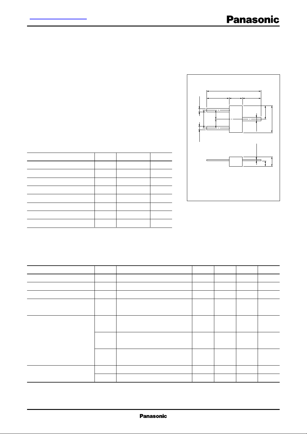
unit: mm
+0.2
5.8
−0.3
+0.25
1.5
2.4±0.1 1.9±0.1
+0.1
−0.05
0.4
0.95
1.9±0.2
0.95
+0.1
−0.05
0.4
−0.05
1
3
2
Mini Flat Package (3-pin)
+0.1
−0.05
0.4
+0.1
−0.06
0.16
1.45
+0.2
+0.2
−0.1
0.8
1.1
1: Drain
2: Source
3: Gate
−0.05
2.9
Marking Symbol: 1H
Note: For the forming type, (Y) is indicated after the part No.
■ Electrical Characteristics (Ta = 25°C)
Parameter
Current consumption
Drain to Source cut-off current
Mutual conductance
Noise figure
Voltage gain
Voltage gain difference
Symbol
I
D
I
DSS
g
m
NV
G
V1
G
V2
G
V3
∆|GV2 − GV1|
∆|GV1 − GV3|
VD = 4.5V, CO = 10pF, RD = 2.2kΩ ± 1%
VDS = 4.5V, VGS = 0
VD = 4.5V, VGS = 0, f = 1kHz
VD = 4.5V, RD = 2.2kΩ ± 1%
CO = 10pF, A-curve
VD = 4.5V, RD = 2.2kΩ ± 1%
CO = 10pF, eG = 10mV, f = 1kHz
VD = 12V, RD = 2.2kΩ ± 1%
CO = 10pF, eG = 10mV, f = 1kHz
VD = 1.5V, RD = 2.2kΩ ± 1%
CO = 10pF, eG = 10mV, f = 1kHz
Conditions
min
100
95
0.7
−3
0
−4.5
0
0
typ
1.6
2
3.3
− 0.3
max
600
480
4
+3.5
+3.5
Unit
µA
µA
mS
µV
dB
dB
dB
dB
dB
1
Page 2
Silicon Junction FETs (Small Signal)
2SK123
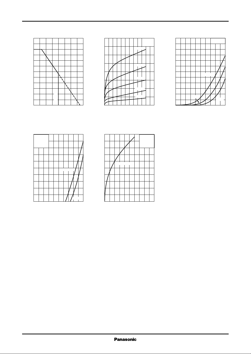
PD Ta ID V
240
)
mW
(
200
D
160
120
80
40
Allowable power dissipation P
0
0 16040 12080 14020 10060
Ambient temperature Ta (˚C
2.0
V
=4.5V
DS
f=1kHz
Ta=25˚C
)
1.6
mS
(
m
1.2
0.8
max.
opr
T
gm V
I
DSS
GS
=0.3mA
DS
0.40
0.35
)
0.30
mA
(
0.25
D
0.20
0.15
Drain current I
0.10
0.05
0
012108264
)
Drain to source voltage VDS (V
gm I
2.0
)
1.6
mS
(
m
1.2
0.8
I
DSS
=0.3mA
VGS=0V
– 0.05V
– 0.10V
– 0.15V
– 0.20V
D
Ta=25˚C
V
=4.5V
DS
f=1kHz
Ta=25˚C
)
600
500
)
µA
(
400
D
300
200
Drain current I
100
0
– 0.5 0– 0.1– 0.4 – 0.2– 0.3
Gate to source voltage VGS (V
ID V
25˚C
GS
Ta=75˚C
=4.5V
V
DS
–25˚C
)
0.4
Mutual conductance g
0
–1.0 0– 0.2– 0.8 – 0.4– 0.6
Gate to source voltage VGS (V
0.15mA
0.4
Mutual conductance g
)
0
0 0.50.40.1 0.30.2
Drain current ID (mA
)
2
 Loading...