

Panasonic 2SK1228 Datasheet
Silicon MOS FETs (Small Signal)
2SK1228
Silicon N-Channel MOS FET
For switching
■ Features
●High-speed switching
●Wide frequency band
●Incorporating a built-in gate protection-diode
●Allowing 2.5V drive
■ Absolute Maximum Ratings (Ta = 25°C)
Parameter
Drain to Source voltage
Gate to Source voltage
Drain current
Max drain current
Allowable power dissipation
Channel temperature
Storage temperature
Symbol
V
DS
V
GSO
I
D
I
DP
P
D
T
ch
T
stg
Ratings
50
10
50
100
150
150
−55 to +150
■ Electrical Characteristics (Ta = 25°C)
Parameter
Drain to Source cut-off current
Gate to Source leakage current
Drain to Source breakdown voltage
Gate threshold voltage
Drain to Source ON-resistance
Forward transfer admittance
Input capacitance (Common Source)
Output capacitance (Common Source)
Reverse transfer capacitance (Common Source)
Turn-on time
Turn-off time
1
*
Pulse measurement
2
*
ton, t
measurement circuit
off
V
out
470Ω
= 2.5V
V
GS
50Ω
100µF
V
DD
Symbol
I
DSS
I
GSS
V
DSS
V
th
R
DS(on)
| Yfs |
C
iss
C
oss
C
rss
t
on
t
off
= 5V
VDS = 20V, VGS = 0
VGS = 10V, VDS = 0
ID = 10µA, VGS = 0
ID = 100µA, VDS = 5V
1
*
ID = 10mA, VGS = 2.5V
ID = 10mA, VDS = 5V, f = 1kHz
VDS = 5V, VGS = 0, f = 1MHz
2
*
VDD = 5V, VGS = 0 to 2.5V, RL = 470Ω
2
*
VDD = 5V, VGS = 2.5 to 0V, RL = 470Ω
V
in
V
out
Unit
mA
mA
mW
Conditions
90%
10%
°C
°C
V
V
10%
90%
+0.2
2.8
–0.3
+0.25
1.5
0.65±0.15 0.65±0.15
1
0.950.95
+0.2
–0.05
2.9
1.9±0.2
2
+0.2
–0.1
0.8
1.1
0.1 to 0.3
0.4±0.2
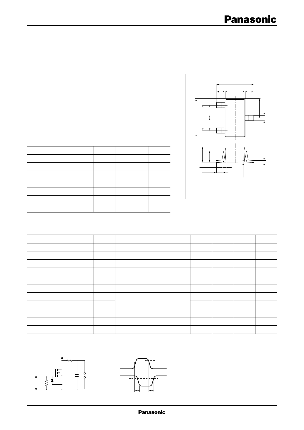
1: Gate JEDEC: TO-236
2: Source EIAJ: SC-59
3: Drain Mini Type Package (3-pin)
–0.05
unit: mm
1.45
3
+0.1
+0.1
0 to 0.1
Marking Symbol: 4V
min
50
0.5
20
typ
100
0.8
27
39
4.5
4.1
1.2
0.2
0.2
max
1
1
1.1
50
Unit
–0.05
0.4
–0.06
0.16
µA
µA
V
V
Ω
mS
pF
pF
pF
µs
µs
t
ontoff
1
Silicon MOS FETs (Small Signal)
2SK1228
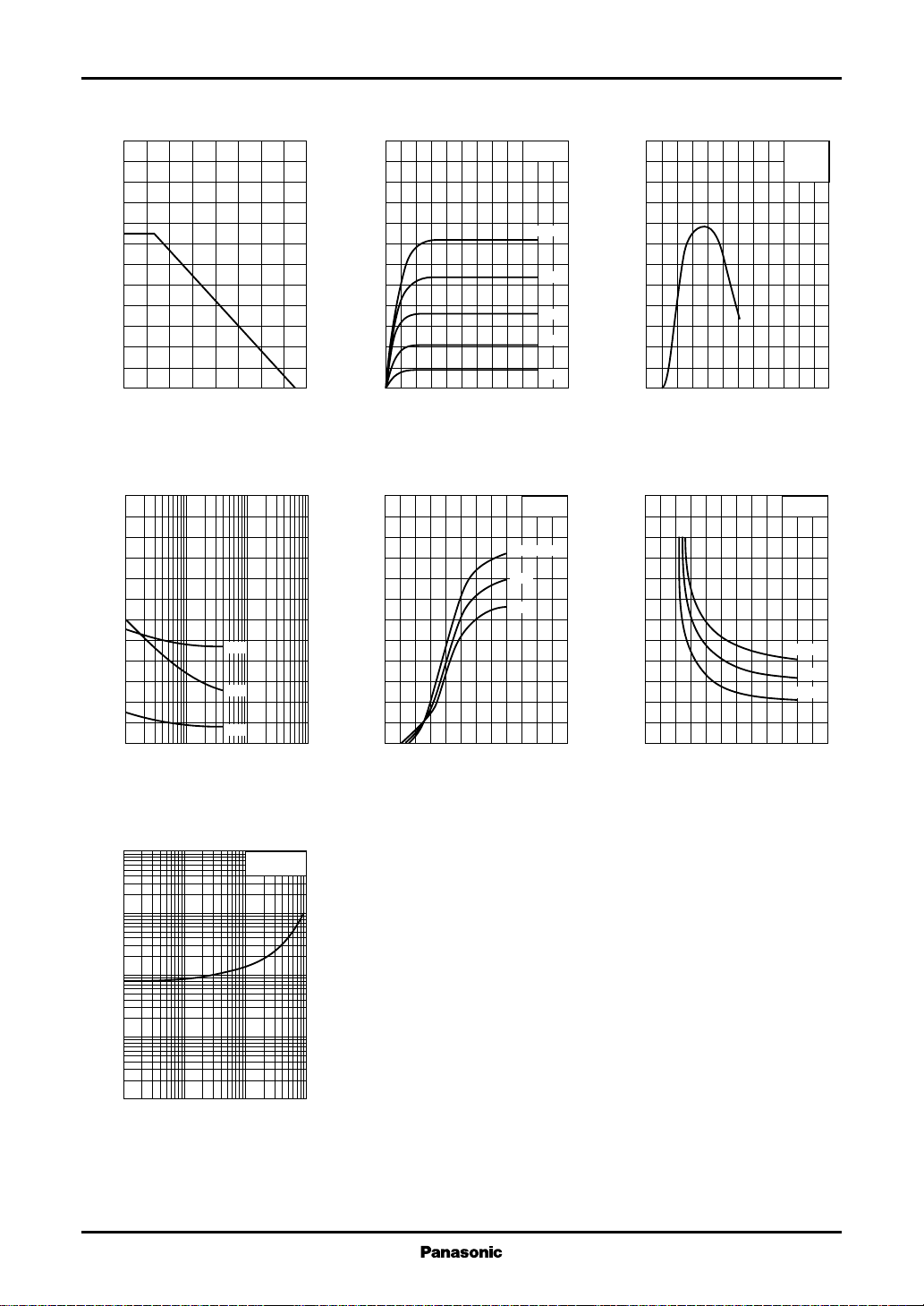
PD Ta ID V
240
)
mW
(
200
D
160
120
80
40
Allowable power dissipation P
0
0 16040 12080 14020 10060
Ambient temperature Ta (˚C
C
, C
, C
iss
oss
rss
12
)
,
)
pF
(
10
rss
,C
Common source
(
oss
,C
8
iss
C
)
6
, Output capacitance
)
Common source
(
4
Common source
(
2
Input capacitance
Reverse transfer capacitance
0
1 10 100 10003 30 300
Drain to source voltage VDS (V
V
C
oss
C
iss
C
rss
DS
DS
48
40
Ta=25˚C
)
mA
(
32
D
24
16
Drain current I
8
0
012108264
)
Drain to source voltage VDS (V
ID V
120
100
)
mA
(
80
D
60
40
GS
VGS=1.8V
1.6V
1.4V
1.2V
1.0V
V
DS
Ta=–25˚C
25˚C
75˚C
)
=5V
60
)
mS
(
50
|
fs
40
30
20
10
Forward transfer admittance |Y
0
120
)
Ω
(
100
DS(on)
80
60
40
Drain current I
20
0
0654132
)
Gate to source voltage VGS (V
)
20
Drain to source ON-resistance R
0
| Yfs | V
0654132
GS
VDS=5V
f=1kHz
Ta=25˚C
Gate to source voltage VGS (V
R
V
DS(on)
0654132
GS
ID=10mA
Ta=75˚C
25˚C
–25˚C
Gate to source voltage VGS (V
)
)
VIN I
100
30
)
10
V
(
IN
3
1
0.3
Input voltage V
0.1
0.03
0.01
0.1 1 10 1000.3 3 30
Output current IO (mA
2
O
VO=5V
Ta=25˚C
)
 Loading...