

Panasonic 2SK0615 Datasheet
Silicon MOS FETs (Small Signal)
2SK615
Silicon N-Channel MOS FET
For switching
■ Features
●Low ON-resistance
●High-speed switching
●Allowing to be driven directly by CMOS and TTL
●M type package, allowing easy automatic and manual insertion as
well as stand-alone fixing to the printed circuit board.
■ Absolute Maximum Ratings (Ta = 25°C)
Parameter
Drain to Source voltage
Gate to Source voltage
Drain current
Max drain current
Allowable power dissipation
Channel temperature
Storage temperature
*
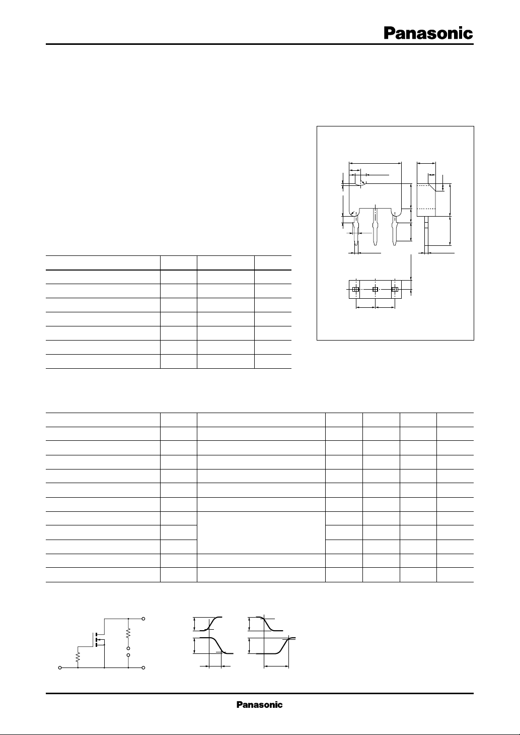
PC board: Copper foil of the drain portion should have a area of 1cm2 or
more and the board thickness should be 1.7mm.
Symbol
V
DS
V
GSO
I
D
I
DP
*
P
D
T
ch
T
stg
Ratings
80
20
±0.5
±1
1
150
−55 to +150
Unit
V
V
A
A
W
°C
°C
■ Electrical Characteristics (Ta = 25°C)
Parameter
Drain to Source cut-off current
Gate to Source leakage current
Drain to Source breakdown voltage
Gate threshold voltage
Drain to Source ON-resistance
Forward transfer admittance
Input capacitance (Common Source)
Output capacitance (Common Source)
Reverse transfer capacitance (Common Source)
Turn-on time
Turn-off time
1
*
Pulse measurement
2
*
ton, t
measurement circuit
off
V
= 10V
in
= 1µS
t
f = 1MHZ
50Ω
68Ω
V
DD
V
out
= 30V
Symbol
I
DSS
I
GSS
V
DSS
V
th
R
DS(on)
| Yfs |
C
iss
C
oss
C
rss
1, 2
*
t
on
1, 2
*
t
off
V
V
Conditions
VDS = 60V, VGS = 0
VGS = 20V, VDS = 0
IDS = 100µA, VGS = 0
ID = 1mA, VDS = V
1
*
ID = 0.5A, VGS = 10V
ID = 0.2A, VDS = 15V, f = 1kHz
VDS = 10V, VGS = 0, f = 1MHz
t
10%
on
90%
V
in
V
out
in
out
GS
10%
t
off
90%
6.9±0.1
1.5
1.5 R0.9
0.4
R0.9
R0.7
1.0±0.1
0.85
0.55±0.1 0.45±0.05
123
2.5 2.5
min
typ
80
1.5
2
300
45
30
8
15
20
unit: mm
2.5±0.1
1.0
1.0
3.5±0.1
2.0±0.2
2.4±0.21.25±0.05
M Type Mold Package
max
10
0.1
4.1±0.2 4.5±0.1
1: Gate
2: Drain
3: Source
EIAJ: SC-71
Unit
µA
µA
V
3.5
4
V
Ω
mS
pF
pF
pF
ns
ns
1
Silicon MOS FETs (Small Signal)
2SK615
PD Ta ID V
1.6
)
1.4
W
(
D
1.2
1.0
0.8
0.6
0.4
0.2
Allowable power dissipation P
0
0 16040 12080 14020 10060
600
)
mS
(
500
|
fs
400
300
200
100
Forward transfer admittance |Y
0
0654132
Copper foil of the drain portion
should have a area of 1cm
or more and the board
thickness should be 1.7mm.
Ambient temperature Ta (˚C
| Yfs | V
GS
Gate to source voltage VGS (V
2
VDS=15V
f=1kHz
Ta=25˚C
)
A
(
D
Drain current I
)
)
,
)
pF
(
rss
,C
Common source
(
oss
,C
iss
C
)
, Output capacitance
)
Common source
(
Common source
(
Input capacitance
Reverse transfer capacitance
)
DS
1.2
1.0
0.8
0.6
0.4
0.2
0
0108264
Drain to source voltage VDS (V
C
, C
, C
oss
rss
V
C
iss
C
oss
C
rss
iss
120
100
80
60
40
20
0
1 10 100 10003 30 300
Drain to source voltage VDS (V
Ta=25˚C
VGS=5.5V
4.5V
3.5V
DS
VGS=0
f=1MHz
Ta=25˚C
ID V
GS
1.2
1.0
)
5V
4V
A
(
0.8
D
0.6
0.4
VDS=10V
Ta=25˚C
Drain current I
3V
)
)
0.2
0
0108264
Gate to source voltage VGS (V
R
V
DS(on)
6
)
Ω
(
5
DS(on)
4
3
2
1
Drain to source ON-resistance R
0
020164128
GS
I
D
Ta=75˚C
25˚C
–25˚C
Gate to source voltage VGS (V
)
=500mA
)
R
Ta
DS(on)
6
)
Ω
(
5
DS(on)
4
V
=5V
3
2
1
Drain to source ON-resistance R
0
–50 7550–25 250
GS
Ambient temperature Ta (˚C
2
ID=500mA
10V
)
 Loading...