

Panasonic 2SK0614 Datasheet
Silicon MOS FETs (Small Signal)
2SK614
Silicon N-Channel MOS FET
For switching
■ Features
●Low ON-resistance R
●High-speed switching
●Allowing to be driven directly by CMOS and TTL
DS(on)
■ Absolute Maximum Ratings (Ta = 25°C)
Parameter
Drain to Source voltage
Gate to Source voltage
Drain current
Max drain current
Allowable power dissipation
Channel temperature
Storage temperature
Symbol
V
DS
V
GSO
I
D
I
DP
P
D
T
ch
T
stg
Ratings
80
20
±0.5
±1
750
150
−55 to +150
■ Electrical Characteristics (Ta = 25°C)
Parameter
Drain to Source cut-off current
Gate to Source leakage current
Drain to Source breakdown voltage
Gate threshold voltage
Drain to Source ON-resistance
Forward transfer admittance
Input capacitance (Common Source)
Output capacitance (Common Source)
Reverse transfer capacitance (Common Source)
Turn-on time
Turn-off time
1
*
Pulse measurement
2
*
ton, t
measurement circuit
off
V
= 10V
in
= 1µS
t
f = 1MHZ
50Ω
68Ω
V
DD
V
out
= 30V
Symbol
I
DSS
I
GSS
V
DSS
V
th
R
DS(on)
| Yfs |
C
iss
C
oss
C
rss
2
*
t
on
2
*
t
off
V
V
VDS = 60V, VGS = 0
VGS = 20V, VDS = 0
IDS = 100µA, VGS = 0
ID = 1mA, VDS = V
1
*
ID = 0.5A, VGS = 10V
ID = 0.2A, VDS = 15V, f = 1kHz
VDS = 10V, VGS = 0, f = 1MHz
in
10%
out
90%
t
on
Conditions
V
in
V
out
Unit
V
V
A
A
mW
°C
°C
GS
t
off
10%
90%
5.1±0.213.5±0.5
1.27 1.27
min
80
1.5
5.0±0.2 4.0±0.2
0.45
2.54±0.15
+0.2
–0.1
213
typ
+0.2
–0.1
0.45
2.3±0.2
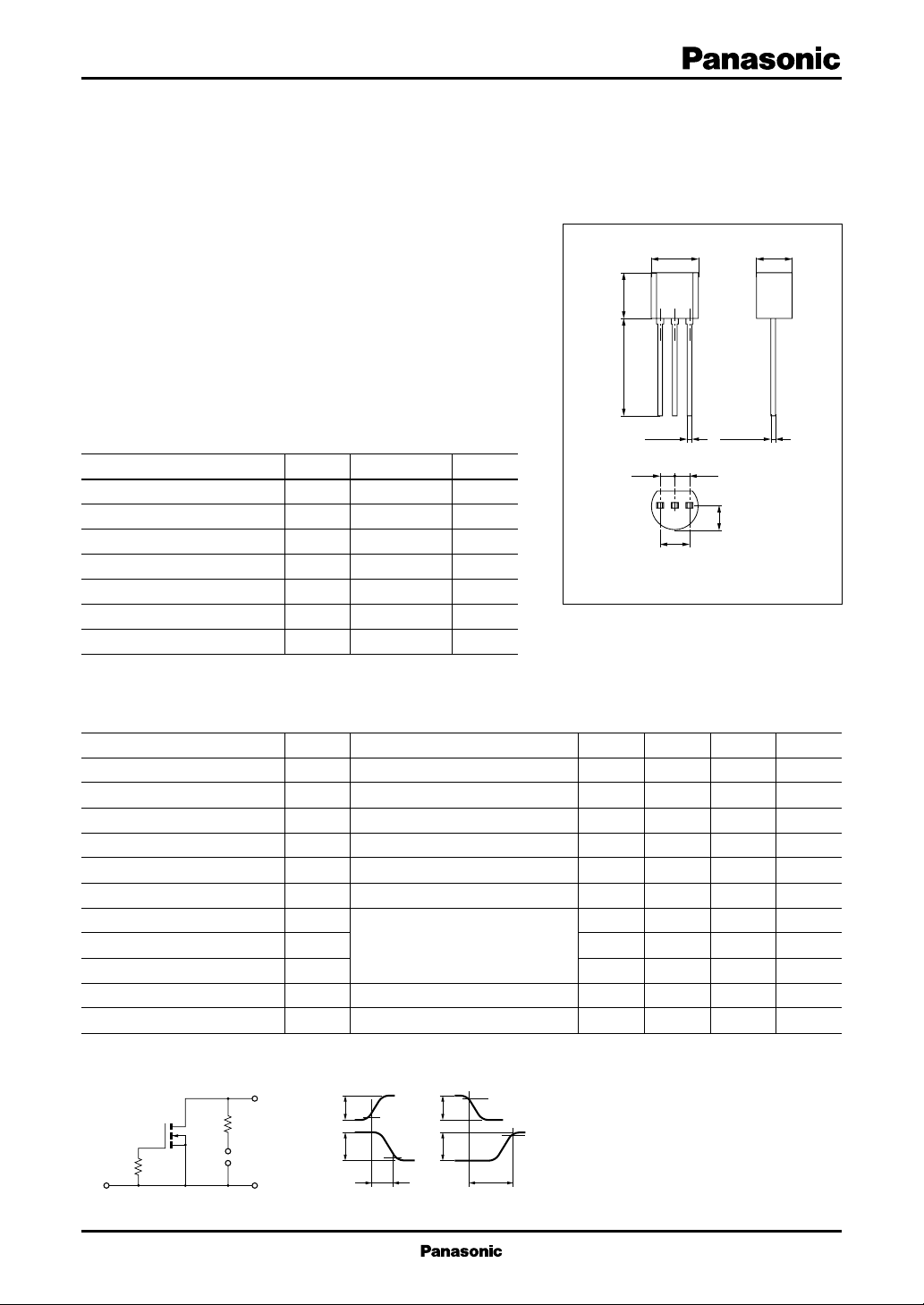
TO-92 Type Package
max
10
0.1
3.5
2
4
300
45
30
8
15
20
unit: mm
1: Source
2: Drain
3: Gate
JEDEC: TO-92
EIAJ: SC-43
Unit
µA
µA
V
V
Ω
mS
pF
pF
pF
ns
ns
1
Silicon MOS FETs (Small Signal)
2SK614
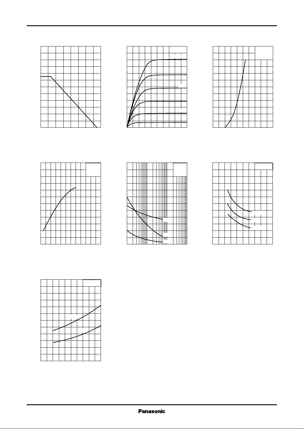
PD Ta ID V
1200
)
mW
(
1000
D
800
600
400
200
Allowable power dissipation P
0
0 16040 12080 14020 10060
Ambient temperature Ta (˚C
| Yfs | V
600
)
mS
(
500
|
fs
400
300
200
100
Forward transfer admittance |Y
0
0654132
Gate to source voltage VGS (V
GS
VDS=15V
f=1kHz
Ta=25˚C
)
A
(
D
Drain current I
)
)
,
)
pF
(
rss
,C
Common source
(
oss
,C
iss
C
)
, Output capacitance
)
Common source
(
Common source
(
Input capacitance
Reverse transfer capacitance
)
DS
1.2
1.0
0.8
0.6
0.4
0.2
0
0108264
Drain to source voltage VDS (V
C
, C
, C
oss
rss
V
C
iss
C
oss
C
rss
iss
120
100
80
60
40
20
0
1 10 100 10003 30 300
Drain to source voltage VDS (V
Ta=25˚C
VGS=5.5V
4.5V
3.5V
DS
VGS=0
f=1MHz
Ta=25˚C
ID V
GS
1.2
1.0
)
5V
4V
A
(
0.8
D
0.6
0.4
VDS=10V
Ta=25˚C
Drain current I
3V
)
)
0.2
0
0108264
Gate to source voltage VGS (V
R
V
DS(on)
6
)
Ω
(
5
DS(on)
4
3
2
1
Drain to source ON-resistance R
0
020164128
GS
I
=500mA
D
Ta=75˚C
25˚C
–25˚C
Gate to source voltage VGS (V
)
)
R
Ta
DS(on)
6
)
Ω
(
5
DS(on)
4
V
=5V
3
2
1
Drain to source ON-resistance R
0
–50 7550–25 250
GS
Ambient temperature Ta (˚C
2
ID=500mA
10V
)
 Loading...