

Panasonic 2SK0301 User Manual
查询2SK0301供应商
Silicon Junction FETs (Small Signal)
2SK0301 (2SK301)
Silicon N-Channel Junction FET
For low-frequency amplification
For switching
■ Features
● Low noies, high gain
● High gate to drain voltage V
GDO
■ Absolute Maximum Ratings (Ta = 25°C)
Parameter
Drain to Source voltage
Gate to Drain voltage
Gate to Source voltage
Drain current
Gate current
Allowable power dissipation
Junction temperature
Storage temperature
Symbol
V
DSX
V
GDO
V
GSO
I
D
I
G
P
D
T
j
T
stg
Ratings
−55 to +125
55
−55
−55
±30
10
250
125
Unit
V
V
V
mA
mA
mW
°C
°C
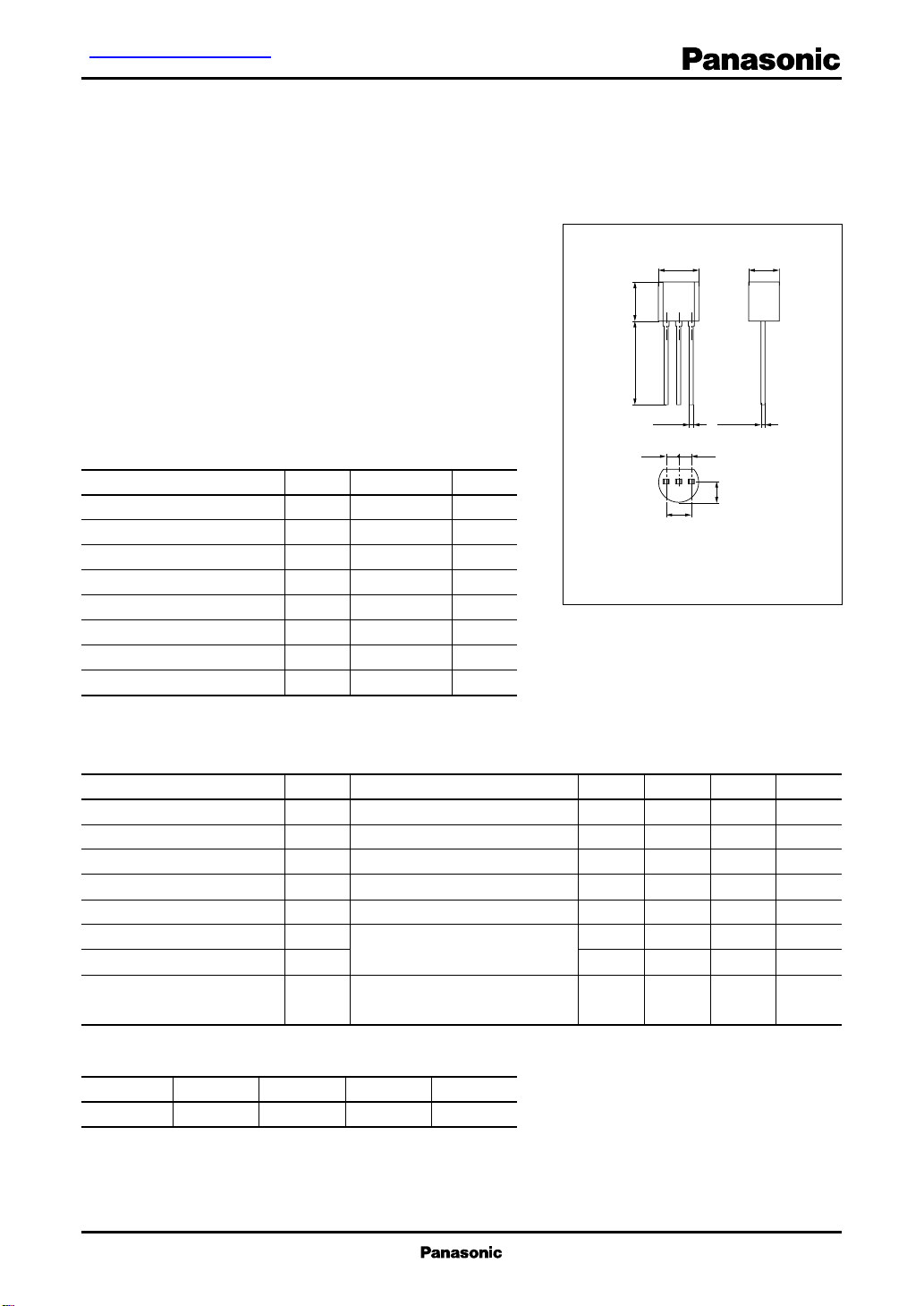
5.0±0.2 4.0±0.2
5.1±0.213.5±0.5
+0.2
–0.1
1.27 1.27
213
2.54±0.15
unit: mm
+0.2
0.45
–0.10.45
2.3±0.2
TO-92 Type Package
1: Drain
2: Gate
3: Source
JEDEC: TO-92
EIAJ: SC-43
■ Electrical Characteristics (Ta = 25°C)
Parameter
Drain to Source cut-off current
Gate to Source leakage current
Gate to Drain voltage
Gate to Source cut-off voltage
Mutual conductance
Input capacitance (Common Source)
Reverse transfer capacitance (Common Source)
Noise figure
*
I
rank classification
DSS
I
Runk
DSS
(mA)
P
1 to 3
Symbol
I
DSS
I
GSS
V
GDC
V
GSC
g
m
C
iss
C
rss
NF
Q
2 to 6.5
*
VDS = 10V, VGS = 0
VGS = −30V, VDS = 0
IG = −100µA, VDS = 0
VDS = 10V, ID = 10µA
VDS = 10V, VGS = 0, f = 1kHz
VDS = 10V, VGS = 0, f = 1MHz
VDS = 10V, VGS = 0, Rg = 100kΩ
f = 100Hz
Conditions
min
1
typ
max
20
−10
−55
−80
−5
2.5
7.5
6.5
1.9
0.5
R
5 to 12
S
10 to 20
Note) The part number in the parenthesis shows conventional part number.
Unit
mA
nA
V
V
mS
pF
pF
dB
247
Silicon Junction FETs (Small Signal)
2SK0301
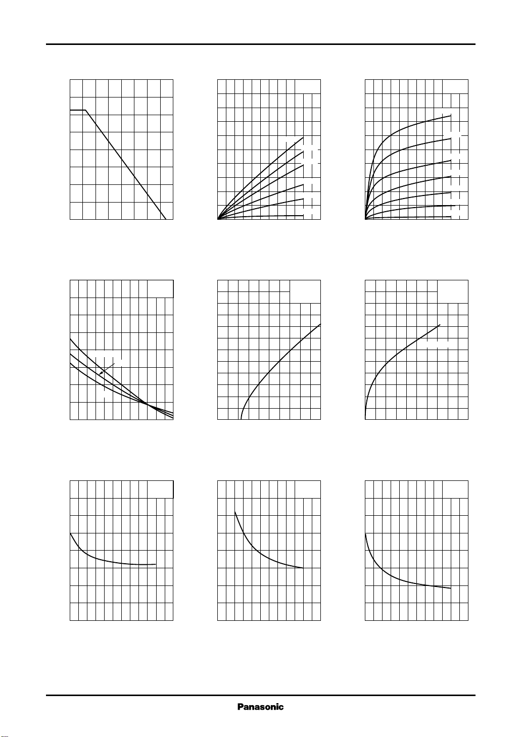
PD Ta ID V
320
)
280
mW
(
D
240
200
160
120
80
40
Allowable power dissipation P
0
0 16040 12080 14020 10060
Ambient temperature Ta (˚C
16
14
)
12
mA
(
10
D
8
Ta=–25˚C
6
Drain current I
4
2
ID V
75˚C
GS
25˚C
VDS=10V
DS
5
4
)
mA
(
3
D
2
Drain current I
1
0
00.60.50.40.1 0.30.2
)
Drain to source voltage VDS (V
gm V
12
)
10
mS
(
m
8
6
4
2
Mutual conductance g
GS
Ta=25˚C
V
=0
GS
– 0.2V
– 0.4V
– 0.6V
– 0.8V
–1.0V
)
VDS=10V
Ta=25˚C
10
8
)
mA
(
6
D
4
Drain current I
2
0
012108264
Drain to source voltage VDS (V
12
)
10
mS
(
m
8
6
4
2
Mutual conductance g
ID V
gm I
I
DSS
DS
D
=7.5mA
Ta=25˚C
VGS=0V
– 0.2V
– 0.4V
– 0.6V
– 0.8V
– 1.0V
– 1.2V
VDS=10V
Ta=25˚C
)
0
0 –1.2–1.0– 0.8– 0.2 – 0.6– 0.4
Gate to source voltage VGS (V
C
V
iss
16
)
pF
(
14
iss
C
)
12
10
8
Common source
(
6
4
2
Input capacitance
0
012108264
Drain to source voltage VDS (V
248
DS
VGS=0
Ta=25˚C
)
)
0
–2.0 0– 0.4–1.6 – 0.8–1.2
Gate to source voltage VGS (V
C
V
oss
)
8
pF
(
7
oss
C
)
6
5
4
Common source
(
3
2
1
Output capacitance
0
012108264
Drain to source voltage VDS (V
DS
VGS=0
Ta=25˚C
0
0108264
)
)
8
pF
(
rss
7
C
)
6
5
Common source
(
4
3
2
1
Reverse transfer capacitance
0
012108264
)
Drain to source voltage VDS (V
Drain current ID (mA
C
V
rss
DS
)
VGS=0
Ta=25˚C
)
 Loading...