

Panasonic 2SK0123 Technical data
查询2SK0123供应商
Silicon Junction FETs (Small Signal)
2SK0123 (2SK123)
Silicon N-Channel Junction FET
For impedance conversion in low frequency
For electret capacitor microphone
■ Features
●High mutual conductance g
●Low noise voltage of NV
■ Absolute Maximum Ratings (T
Parameter
Drain to Source voltage
Drain to Gate voltage
Drain to Source current
Drain to Gate current
Gate to Source current
Allowable power dissipation
Operating ambient temperature
Storage temperature
m
Symbol
V
DSO
V
DGO
I
DSO
I
DGO
I
GSO
P
D
T
opr
T
stg
= 25°C)
a
−20 to +80
−55 to +150
Ratings
20
20
2
2
2
200
Unit
V
V
mA
mA
mA
mW
°C
°C
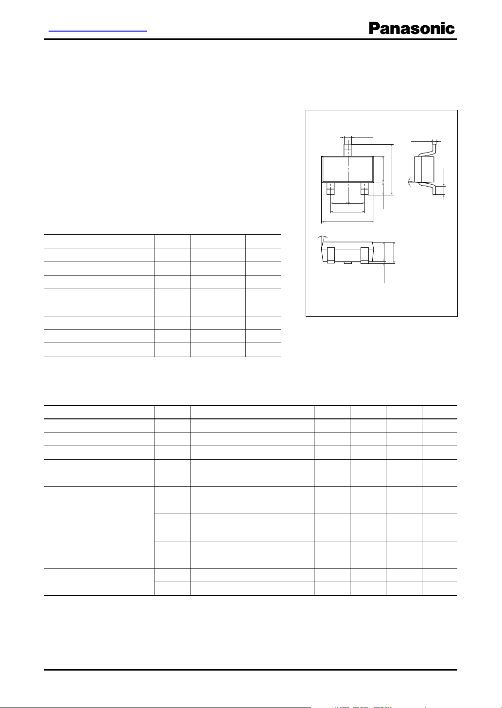
Unit: mm
+0.10
0.40
10˚
3
1
(0.95) (0.95)
±0.1
1.9
+0.20
2.90
–0.05
–0.05
+0.25
–0.05
+0.2
–0.3
2.8
1.50
2
(0.65)
+0.2
–0.1
+0.3
–0.1
1.1
1.1
0 to 0.1
+0.10
0.16
–0.06
5˚
Mini3-G1 Package
0.4±0.2
1: Drain
2: Source
3: Gate
Marking Symbol: 1H
Note: For the forming type, (Y) is indicated after the part No.
■ Electrical Characteristics (T
Parameter
Current consumption
Drain to Source cut-off current
Mutual conductance
Noise figure
Voltage gain
Voltage gain difference
Symbol
I
D
I
DSS
g
m
NV
G
G
G
∆|GV2 − G
∆|GV1 − G
= 25°C)
a
V1
V2
V3
Conditions
V
= 4.5 V, CO = 10 pF, RD = 2.2 kΩ ± 1%
D
V
= 4.5 V, VGS = 0
DS
V
= 4.5 V, VGS = 0, f = 1 kHz
D
V
= 4.5V, RD = 2.2 kΩ ± 1%
D
C
= 10 pF, A-curve
O
V
= 4.5 V, RD = 2.2 kΩ ± 1%
D
C
= 10 pF, eG = 10 mV, f = 1 kHz
O
V
= 12 V, RD = 2.2 kΩ ± 1%
D
C
= 10 pF, eG = 10 mV, f = 1 kHz
O
|
V
= 1.5 V, RD = 2.2 kΩ ± 1%
V1
D
|
C
= 10 pF, eG = 10 mV, f = 1 kHz
V3
O
Note) The part number in the parenthesis shows conventional part number.
min
100
95
0.7
−3
0
−4.5
0
0
typ
1.6
2
3.3
− 0.3
max
600
480
4
+3.5
+3.5
Unit
µA
µA
mS
µV
dB
dB
dB
dB
dB
Publication date: January 2002 SJF00005BED
1

2SK0123
P
T
D
240
)
200
mW
(
D
160
120
80
40
Allowable power dissipation P
0
0 16040 12080 14020 10060
Ambient temperature Ta (°C
2.0
V
DS
f = 1 kHz
= 25°C
T
)
mS
(
a
1.6
m
1.2
0.8
= 4.5 V
g
V
m
max.
opr
T
I
DSS
a
GS
= 0.3 mA
I
V
D
DS
0.40
0.35
0.30
)
mA
(
0.25
D
0.20
0.15
Drain current I
0.10
0.05
0
012108264
)
Drain to source voltage VDS (V
g
I
m
2.0
)
1.6
mS
(
m
1.2
0.8
I
DSS
= 0.3 mA
VGS = 0 V
− 0.05 V
− 0.10 V
− 0.15 V
− 0.20 V
D
V
f = 1 kHz
T
Ta = 25°C
= 4.5 V
DS
= 25°C
a
)
600
500
)
mA
400
(
D
300
200
Drain current I
100
0
− 0.5 0− 0.1− 0.4 − 0.2− 0.3
I
V
D
GS
V
= 4.5 V
DS
Ta = 75°C
25°C
−25°C
Gate to source voltage VGS (V
)
0.4
Mutual conductance g
0
−1.0 0− 0.2− 0.8 − 0.4− 0.6
Gate to source voltage VGS (V
0.15 mA
0.4
Mutual conductance g
0
0 0.50.40.1 0.30.2
)
Drain current ID (mA
)
2
SJF00005BED
 Loading...