

Panasonic 2SK0065 Datasheet
Silicon Junction FETs (Small Signal)
2SK65
Silicon N-Channel Junction FET
For impedance conversion in low frequency
For electret capacitor microphone
■ Features
●Diode is connected between gate and source
●Low noise voltage
■ Absolute Maximum Ratings (Ta = 25°C)
Parameter
Drain to Source voltage
Gate to Drain voltage
Drain to Source current
Drain to Gate current
Gate to Source current
Allowable power dissipation
Operating ambient temperature
Storage temperature
Symbol
V
DSO
V
GDO
I
DSO
I
DGO
I
GSO
P
D
T
opr
T
stg
Ratings
12
−12
2
2
2
20
−10 to +70
−20 to +150
■ Electrical Characteristics (Ta = 25°C)
Parameter
Drain to Source cut-off current
Mutual conductance
Noise figure
Voltage gain
Symbol
*
I
DSS
g
m
NV
*
G
V1
*
G
V2
*
G
V3
VDS = 4.5V, VGS = 0, RS = 2.2kΩ ± 1%
VDS = 4.5V, VGS = 0
RS = 2.2kΩ ± 1%, f = 1kHz
VDS = 4.5V, RS = 2.2kΩ ± 1%
CG = 10pF, A-curve
VDS = 4.5V, RS = 2.2kΩ ± 1%
CG = 10pF, eG = 100mV, f = 70Hz
VDS = 12V, RS = 2.2kΩ ± 1%
CG = 10pF, eG = 100mV, f = 70Hz
VDS = 1V, RS = 2.2kΩ ± 1%
CG = 10pF, eG = 100mV, f = 70Hz
Unit
V
V
mA
mA
mA
mW
°C
°C
Conditions
0.45±0.05
min
0.04
300
4.5±0.1
123
typ
500
−10
−9.5
−11
4.0±0.210.5±0.5
max
0.8
4
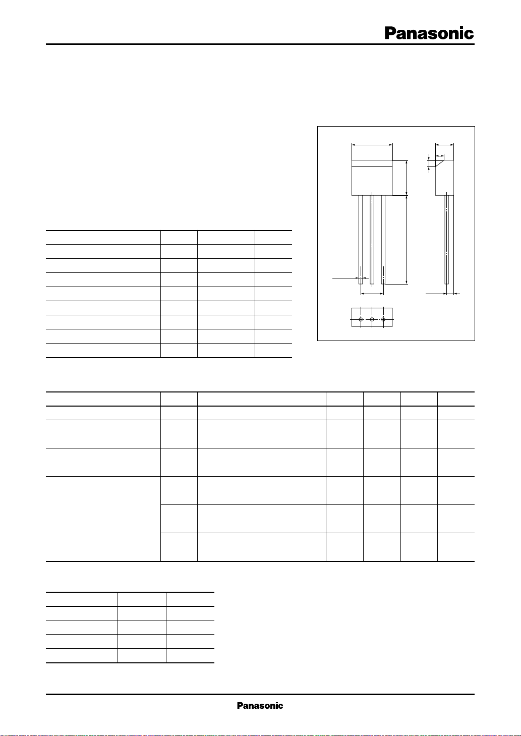
unit: mm
2.0±0.2
1.0
0.7
0.8±0.12.54
1: Drain
2: Gate
3: Source
S Type Package
Unit
mA
µS
µV
dB
dB
dB
*
I
rank classification and GV value
DSS
Runk
I
DSS
(mA)
0.04 to 0.2
GV1 (dB)
GV2 (dB)
∆| GV1 − GV2 | (dB)
P
> −13
> −12
< 3
Q
0.15 to 0.8
> −12
> −11
< 3
1
Silicon Junction FETs (Small Signal)
2SK65
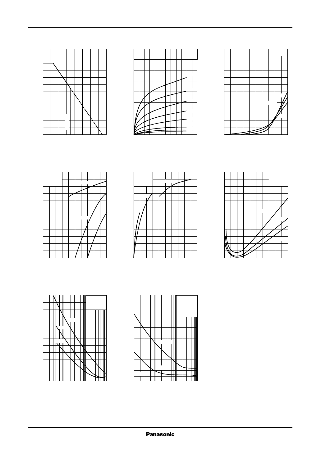
PD Ta ID V
24
)
mW
(
20
D
16
12
8
4
Allowable power dissipation P
0
0 16040 12080 14020 10060
Ambient temperature Ta (˚C
1.2
VDS=4.5V
f=1kHz
Ta=25˚C
)
1.0
mS
(
m
0.8
0.6
0.4
0.2
Mutual conductance g
max.
opr
T
gm V
I
DSS
0.3mA
GS
=0.9mA
0.1mA
DS
800
700
)
600
µA
(
500
D
400
300
Drain current I
200
100
0
012108264
)
Drain to source voltage VDS (V
gm I
1.2
VDS=4.5V
)
mS
(
f=1kHz
Ta=25˚C
1.0
0.3mA
m
0.8
0.1mA
0.6
0.4
I
DSS
=0.9mA
Ta=25˚C
VGS=0V
– 0.1V
– 0.2V
– 0.3V
– 0.4V
– 0.5V
– 0.6V
– 0.7V
)
D
1.2
1.0
)
mA
(
0.8
D
0.6
0.4
Drain current I
0.2
0
–2.0 0– 0.4–1.6 – 0.8–1.2
Gate to source voltage VGS (V
24
20
)
dB
(
16
12
8
Noise figure NF
0.2
Mutual conductance g
4
ID V
NF I
GS
Ta=–25˚C
25˚C
D
f=100Hz
=4.5V
V
DS
75˚C
VDS=4.5V
=100kW
R
g
Ta=25˚C
1kHz
10kHz
)
0
–1.0 0– 0.2– 0.8 – 0.4– 0.6
Gate to source voltage VGS (V
NF R
24
20
)
dB
(
16
12
8
f=100Hz
1kHz
10kHz
Noise figure NF
4
0
0.1 1 10 1000.3 3 30
Signal source resistance Rg (kΩ
2
g
VDS=4.5V
I
=300µA
D
Ta=25˚C
)
)
0
0 1.00.80.2 0.60.4
Drain current ID (mA
NF f
16
14
)
12
dB
(
10
8
6
Noise figure NF
4
2
1000kΩ
0
0.01 0.1 1 100.03 0.3 3
R
=10kΩ
g
100kΩ
Frequency f (KHz
)
VDS=4.5V
=300µA
I
D
Ta=25˚C
)
0
0 1.00.80.2 0.60.4
Drain current ID (mA
)
 Loading...