

4.0±0.2
marking
2.54±0.15
1.271.27
3.0±0.215.6±0.5
2.0±0.2
0.7±0.1
0.45
–
0.1
123
+0.2
查询2SJ164供应商
Silicon Junction FETs (Small Signal)
2SJ164
Silicon P-Channel Junction FET
For switching
Complementary to 2SK1104
■ Features
●Low ON-resistance
●Low-noise characteristics
■ Absolute Maximum Ratings (Ta = 25°C)
Parameter
Gate to Drain voltage
Drain current
Gate current
Allowable power dissipation
Channel temperature
Storage temperature
Symbol
V
GDS
I
D
I
G
P
D
T
ch
T
stg
Ratings
65
−20
−10
300
150
−55 to +150
■ Electrical Characteristics (Ta = 25°C)
Parameter
Drain to Source cut-off current
Gate to Source leakage current
Gate to Drain voltage
Gate to Source cut-off voltage
Forward transfer admittance
Drain to Source ON-resistance
Input capacitance (Common Source)
Output capacitance (Common Source)
Reverse transfer capacitance (Common Source)
Symbol
*
I
DSS
I
GSS
V
GDS
V
GSC
| Yfs |
R
DS(on)
C
iss
C
oss
C
rss
VDS = −10V, VGS = 0
VGS = 30V, VDS = 0
IG = 10µA, VDS = 0
VDS = −10V, ID = −10µA
VDS = −10V, ID = −1mA, f = 1kHz
VDS = −10mV, VGS = 0
VDS = −10V, VGS = 0, f = 1MHz
Unit
V
mA
mA
mW
°C
°C
Conditions
min
− 0.2
65
1.8
typ
1.5
2.5
300
10
3
3
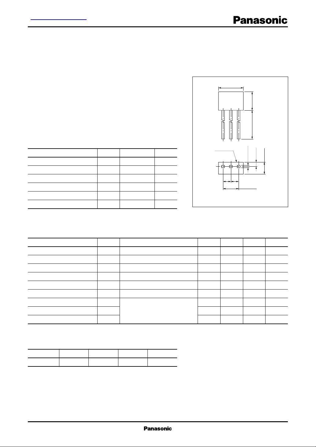
unit: mm
1: Source
2: Gate
3: Drain
EIAJ: SC-72
New S Type Package
max
−6
10
Unit
mA
nA
V
3.5
V
mS
Ω
pF
pF
pF
*
I
rank classification
DSS
Runk
I
(mA)O− 0.2 to −1P− 0.6 to −1.5Q−1 to −3R−2.5 to −6
DSS
1
Silicon Junction FETs (Small Signal)
2SJ164
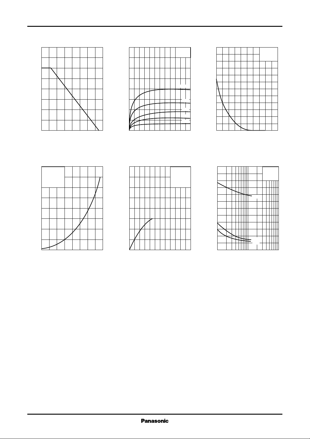
PD Ta ID V
200
)
175
mW
(
D
150
125
100
75
50
25
Allowable power dissipation P
0
0 16040 12080 14020 10060
Ambient temperature Ta (˚C
| Yfs | V
4.0
)
VDS=–10V
mS
3.5
f=1kHz
(
Ta=25˚C
|
fs
3.0
2.5
2.0
1.5
1.0
0.5
Forward transfer admittance |Y
0
2.0 01.5 0.51.0
Gate to source voltage VGS (V
GS
DS
–4.0
–3.5
)
–3.0
mA
(
–2.5
D
–2.0
–1.5
Drain current I
–1.0
– 0.5
0
0 –12–10–8–2 –6–4
)
Drain to source voltage VDS (V
| Yfs | I
16
)
mS
14
(
|
fs
12
10
8
6
4
2
Forward transfer admittance |Y
0
0 –12–10–8–2 –6–4
)
Drain current ID (mA
D
Ta=25˚C
VGS=0V
0.2V
0.4V
0.6V
0.8V
VDS=–10V
f=1kHz
Ta=25˚C
)
)
–3.0
–2.5
)
mA
(
–2.0
D
–1.5
–1.0
Drain current I
– 0.5
0
054132
Gate to source voltage VGS (V
24
)
,
)
pF
(
20
rss
,C
Common source
(
oss
,C
16
iss
C
)
12
, Output capacitance
)
Common source
(
8
Common source
(
4
Input capacitance
Reverse transfer capacitance
0
–1 –3 –10 –30 –100
Drain to source voltage VDS (V
ID V
GS
VDS=–10V
Ta=25˚C
)
C
, C
, C
oss
rss
V
C
iss
C
oss
C
rss
DS
f=1MHz
=0
V
GS
Ta=25˚C
iss
)
2
 Loading...