

Silicon MOS FETs (Small Signal)
2SJ0536
Silicon P-Channel MOS FET
Secondary battery pack (Li ion battery, etc.)
For switching
■ Features
●High-speed switching
●S-mini type package, allowing downsizing of the sets and auto-
matic insertion through the tape/magazine packing.
●Low-voltage drive (V
: −1 to 2V)
th
●Low Ron
■ Absolute Maximum Ratings (Ta = 25°C)
Parameter
Drain to Source voltage
Gate to Source voltage
Drain current
Max drain current
Allowable power dissipation
Channel temperature
Storage temperature
Symbol
V
DS
V
GSO
I
D
I
DP
P
D
T
ch
T
stg
Ratings
−30
±20
−100
−200
150
150
−55 to +150
Unit
V
V
mA
mA
mW
°C
°C
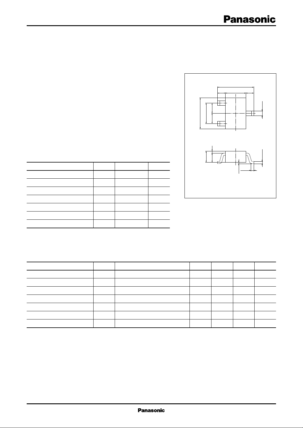
unit: mm
2.1±0.1
1.25±0.1 0.4250.425
–0
1
1.3±0.10.9±0.1
2.0±0.2
0.650.2 0.65
2
0.7±0.1
0.2±0.1
0 to 0.1
1: Gate
2: Source EIAJ: SC-70
3: Drain S-Mini Type Package (3-pin)
+0.1
0.3
3
–0.05
+0.1
0.15
Marking Symbol: 2C
■ Electrical Characteristics (Ta = 25°C)
Parameter
Drain current
Gate cut-off current
Gate threshold voltage
Forward transfer admittance
Drain to source ON-resistance
Turn-on time
Turn-off time
Symbol
I
DSS
I
GSS
V
th
| Yfs |
R
DS(on)
t
on
t
off
VDS = −30V, VGS = 0
VGS = ±20V, VDS = 0
VDS = −5V, ID = −1µA
VDS = −5V, ID = −10mA
VGS = −5V, ID = −10mA
VDD = −5V, VGS = −5 to 0V, RL = 200Ω
VDD = −5V, VGS = −5 to 0V, RL = 200Ω
Conditions
min
−1
8
typ
50
100
25
max
− 0.1
±1
−2
75
Unit
µA
µA
V
mS
Ω
µs
µs
1
Silicon MOS FETs (Small Signal)
2SJ0536
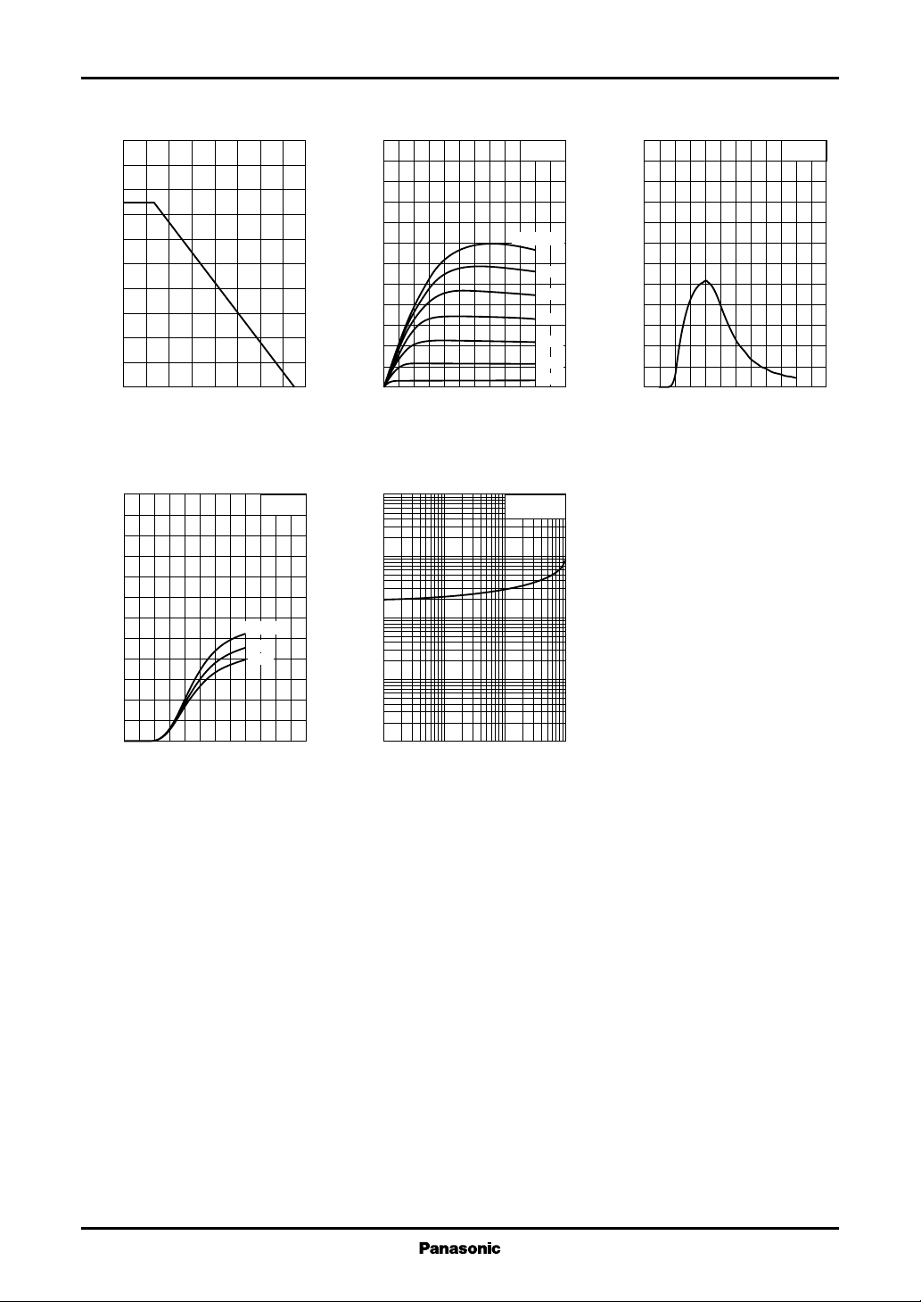
PD Ta ID V
200
)
mW
(
160
D
120
80
40
Allowable power dissipation P
0
0 16040 12080 14020 10060
Ambient temperature Ta (˚C
ID V
GS
–240
–200
)
mA
(
–160
D
–120
–80
Drain current I
–40
0
0 –12–10–8–2 –6–4
Gate to source voltage VGS (V
Ta=–25˚C
25˚C
75˚C
VDS=–5V
DS
–120
–100
Ta=25˚C
)
mA
(
–80
D
–60
–40
Drain current I
–20
0
0 –12–10–8–2 –6–4
)
Drain to source voltage VDS (V
VIN I
–100
–30
)
–10
V
(
IN
–3
–1
– 0.3
Input voltage V
– 0.1
– 0.03
– 0.01
– 0.1 –1 –10 –100– 0.3 –3 –30
)
Output current IO (mA
O
VGS=–5.5V
–5.0V
–4.5V
–4.0V
–3.5V
–3.0V
–2.5V
VO=–5V
Ta=25˚C
)
)
60
)
mS
(
50
|
fs
40
30
20
10
Forward transfer admittance |Y
0
| Yfs | V
0 –12–10–8–2 –6–4
GS
VDS=–5V
Gate to source voltage VGS (V
)
2
 Loading...