

Panasonic 2SD2565 Datasheet
Transistor
2SD2565
Silicon NPN triple diffusion planer type
For high voltage-withstand switching
Features
■
●
High collector to base voltage V
●
High collector to emitter voltage V
●
Large collector power dissipation PC.
●
Low collector to emitter saturation voltage V
●
M type package allowing easy automatic and manual insertion as
well as stand-alone fixing to the printed circuit board.
Absolute Maximum Ratings (Ta=25˚C)
■
Parameter
Collector to base voltage
Collector to emitter voltage
Emitter to base voltage
Peak collector current
Collector current
Collector power dissipation
Junction temperature
Storage temperature
*1
Printed circuit board: Copper foil area of 1cm2 or more, and the board
thickness of 1.7mm for the collector portion
Symbol
V
V
V
I
CP
I
C
P
C
T
j
T
stg
CBO
CEO
EBO
*1
CBO
CEO
.
.
Ratings
400
400
5
1
0.5
1
150
–55 ~ +150
CE(sat)
.
Unit
V
V
V
A
A
W
˚C
˚C
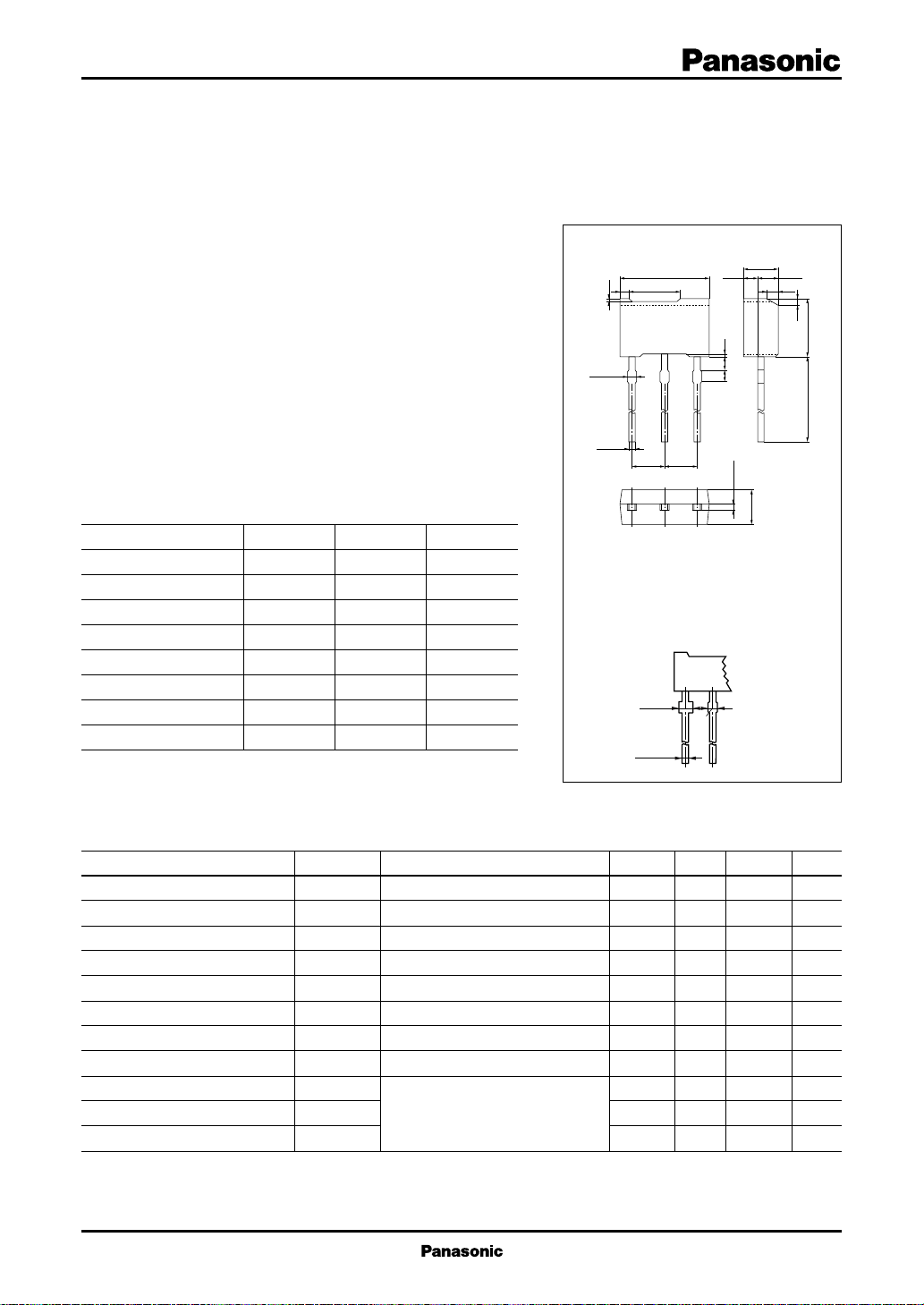
6.9±0.1
4.00.7 0.8
0.15
0.65 max.
+0.1
0.45
–0.05
2.5±0.5 2.5±0.5
Note: In addition to the
lead type shown in
the upper figure, the
type as shown in
the lower figure is
also available.
1.2±0.1
+
0.1
0.45
–
0.05
1.05
±0.05 (1.45)
0.21.01.0
–0.05
+0.1
321
0.45
1:Emitter
2:Collector
3:Base
MT2 Type Package
0.65
max.
Unit: mm
2.5±0.1
0.5
4.5±0.114.5±0.5
2.5±0.1
(HW type)
Electrical Characteristics (Ta=25˚C)
■
Parameter
Collector to base voltage
Collector to emitter voltage
Emitter to base voltage
Forward current transfer ratio
Collector to emitter saturation voltage
Base to emitter saturation voltage
Transition frequency
Collector output capacitance
Turn-on time
Storage time
Fall time
Symbol
V
CBO
V
CEO
V
EBO
h
FE
V
CE(sat)
V
BE(sat)
f
T
C
ob
t
on
t
stg
t
f
Conditions
IC = 100µA, IE = 0
IC = 500µA, IB = 0
IE = 100µA, IC = 0
VCE = 5V, IC = 30mA
IC = 250mA, IB = 50mA
IC = 250mA, IB = 50mA
*
*
VCB = 30V, IE = –20mA, f = 200MHz
VCB = 30V, IE = 0, f = 1MHz
IC = 100mA
IB1 = 10mA, IB2 = –10mA
VCC = 200V
min
400
400
5
30
typ
max
1.5
1.5
30
6
20
0.8
3.7
0.6
*
Pulse measurement
Unit
V
V
V
–
V
V
MHz
pF
µS
µS
µS
1
Transistor
2SD2565
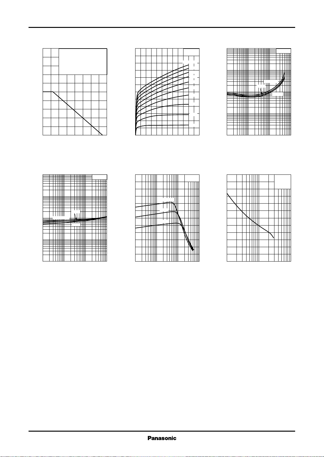
PC — Ta IC — V
2.0
)
W
(
1.6
C
1.2
0.8
0.4
Collector power dissipation P
0
100
)
V
(
30
BE(sat)
10
3
1
0.3
0.1
0.03
Base to emitter saturation voltage V
0.01
Printed circut board: Copper
foil area of 1cm
the board thickness of 1.7mm
for the collector portion.
0 16040 12080 14020 10060
2
or more, and
Ambient temperature Ta (˚C
V
— I
BE(sat)
Ta=–25˚C
1 10 100 10003 30 300
C
IC/IB=5
25˚C
75˚C
Collector current IC (mA
V
CE
)
300
250
)
mA
(
200
C
150
100
Collector current I
50
0
012108264
)
Collector to emitter voltage VCE (V
hFE — I
60
FE
50
40
30
20
10
Forward current transfer ratio h
Ta=75˚C
25˚C
–25˚C
Ta=25˚C
IB=10mA
9mA
8mA
7mA
6mA
5mA
4mA
3mA
2mA
1mA
)
C
VCE=5V
10
V
(
3
CE(sat)
1
0.3
0.1
0.03
0.01
0.003
0.001
Collector to emitter saturation voltage V
1 10 100 10003 30 300
Collector current IC (mA
24
)
pF
(
20
ob
16
12
8
4
— I
CE(sat)
25˚C
Cob — V
C
Ta=75˚C
CB
IC/IB=5
–25˚C
f=1MHz
I
=0
E
Ta=25˚C
)
Collector output capacitance C
0
1 10 100 10003 30 300
)
Collector current IC (mA
)
0
1 3 10 30 100
Collector to base voltage VCB (V
)
2
 Loading...