

Panasonic 2SD2468 Datasheet
Po wer Transistors
2SD2468
Silicon NPN epitaxial planar type
For power switching
Features
■
●
Low collector to emitter saturation voltage V
●
Satisfactory linearity of foward current transfer ratio h
●
Large collector current I
●
Full-pack package with outstanding insulation, which can be in-
C
stalled to the heat sink with one screw
Absolute Maximum Ratings (T
■
Parameter
Collector to base voltage
Collector to emitter voltage
Emitter to base voltage
Peak collector current
Collector current
Collector power
dissipation
TC=25°C
Ta=25°C
Junction temperature
Storage temperature
Symbol
V
CBO
V
CEO
V
EBO
I
CP
I
C
P
C
T
j
T
stg
CE(sat)
=25˚C)
C
Ratings
130
80
7
8
4
35
2
150
–55 to +150
FE
Unit
W
˚C
˚C
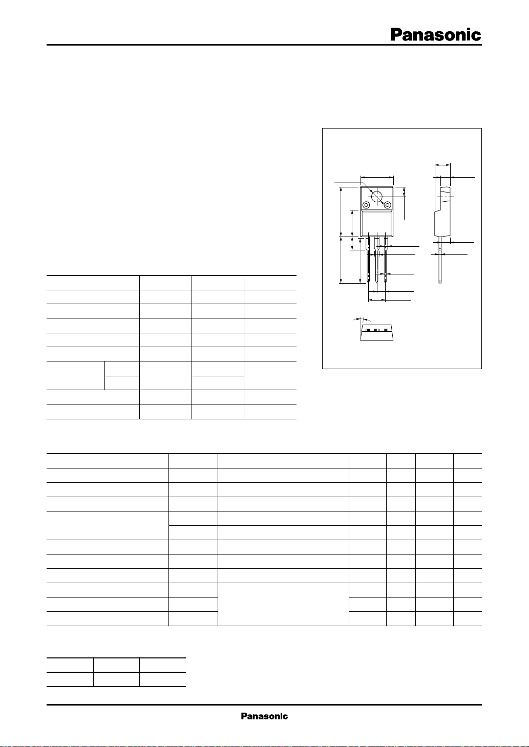
Unit: mm
4.6±0.2
15.0±0.313.7
–0.2
8.0±0.2
4.1±0.2
Solder Dip
7°
9.9±0.3
3.0±0.2
1.2±0.15
1.45±0.15
0.75±0.1
2.54±0.2
5.08±0.4
231
φ3.2±0.1
+0.5
V
V
V
A
A
TO–220E Full Pack Package
2.9±0.2
2.6±0.1
0.7±0.1
1:Base
2:Collector
3:Emitter
Electrical Characteristics (T
■
Parameter
Collector cutoff current
Emitter cutoff current
Collector to emitter voltage
Forward current transfer ratio
Collector to emitter saturation voltage
Base to emitter saturation voltage
Transition frequency
Turn-on time
Storage time
Fall time
*
h
Rank classification
FE2
Rank Q P
h
FE2
90 to 180 130 to 260
C
Symbol
I
CBO
I
EBO
V
CEO
h
FE1
*
h
FE2
V
CE(sat)
V
BE(sat)
f
T
t
on
t
stg
t
f
=25˚C)
Conditions
VCB = 100V, IE = 0
VEB = 5V, IC = 0
IC = 10mA, IB = 0
VCE = 2V, IC = 0.1A
VCE = 2V, IC = 1A
IC = 3A, IB = 0.15A
IC = 3A, IB = 0.15A
VCE = 10V, IC = 0.5A, f = 10MHz
IC = 1A, IB1 = 0.1A, IB2 = – 0.1A,
VCC = 50V
min
80
45
90
typ
30
0.5
2.5
0.15
max
10
50
260
0.5
1.5
Unit
µA
µA
V
V
V
MHz
µs
µs
µs
1
Po wer Transistors 2SD2468
PC—Ta IC—V
50
)
W
(
40
C
(1)
30
20
(2)
10
(3)
Collector power dissipation P
(4)
0
0 16040 12080 14020 10060
Ambient temperature Ta (˚C
100
)
V
(
30
BE(sat)
10
3
1
0.3
0.1
0.03
Base to emitter saturation voltage V
0.0.1
0.01 0.1 1 100.03 0.3 3
(1) TC=Ta
(2) With a 100 × 100 × 2mm
Al heat sink
(3) With a 50 × 50 × 2mm
Al heat sink
(4) Without heat sink
(P
=2W)
C
V
BE(sat)—IC
TC=100˚C
–25˚C
25˚C
Collector current IC (A
IC/IB=20
)
CE
)
8
7
)
6
A
(
C
5
4
3
2
Collector current I
1
0
012108264
)
Collector to emitter voltage VCE (V
IB=300mA
140mA
hFE—I
10000
3000
FE
1000
300
TC=100˚C
25˚C
100
Forward current transfer ratio h
–25˚C
30
10
3
1
0.01 0.1 1 100.03 0.3 3
Collector current IC (A
120mA
C
T
100mA
=25˚C
C
60mA
40mA
20mA
10mA
VCE=2V
)
)
10
V
(
CE(sat)
0.3
0.1
0.03
0.01
0.003
0.001
Collector to emitter saturation voltage V
10000
3000
)
MHz
1000
(
T
300
100
30
10
Transition frequency f
V
CE(sat)—IC
3
1
0.01 0.1 1 100.03 0.3 3
TC=100˚C
25˚C
Collector current IC (A
fT—I
C
VCE=10V
f=10MHz
T
C
3
1
0.01 0.1 1 100.03 0.3 3
Collector current IC (A
IC/IB=20
–25˚C
)
=25˚C
)
Cob—V
10000
)
pF
3000
(
ob
1000
300
100
30
10
3
Collector output capacitance C
1
0.1 1 10 1000.3 3 30
Collector to base voltage VCB (V
2
CB
IE=0
f=1MHz
=25˚C
T
C
)
ton, t
100
30
)
µs
(
10
f
,t
stg
3
,t
on
1
0.3
0.1
Switching time t
0.03
0.01
054132
Collector current IC (A
, tf — I
stg
t
stg
t
f
t
on
C
Pulsed tw=1ms
Duty cycle=1%
=10 (IB1=–IB2)
I
C/IB
=50V
V
CC
T
=25˚C
C
Area of safe operation (ASO)
100
30
)
I
CP
10
A
(
I
C
C
3
1
0.3
0.1
Collector current I
0.03
0.01
1 10 100 10003 30 300
)
Collector to emitter voltage VCE (V
1ms
Non repetitive pulse
=25˚C
T
C
t=0.5ms
DC
10ms
)
 Loading...