

Panasonic 2SC5516 Datasheet
Po wer Transistors
2SC5516
Silicon NPN triple diffusion mesa type
For horizontal deflection output
Features
■
●
High breakdown voltage, and high reliability through the use of a
glass passivation layer
●
High-speed switching
●
Wide area of safe operation (ASO)
Absolute Maximum Ratings (T
■
Parameter
Collector to base voltage
Collector to emitter voltage
Emitter to base voltage
Peak collector current
Collector current
Base current
Collector power
dissipation
TC=25°C
Ta=25°C
Junction temperature
Storage temperature
Symbol
V
V
V
V
I
CP
I
C
I
B
P
C
T
j
T
stg
CBO
CES
CEO
EBO
=25˚C)
C
Ratings
1500
1500
600
5
30
20
8
70
3.5
150
–55 to +150
Unit
V
V
V
V
A
A
A
W
˚C
˚C
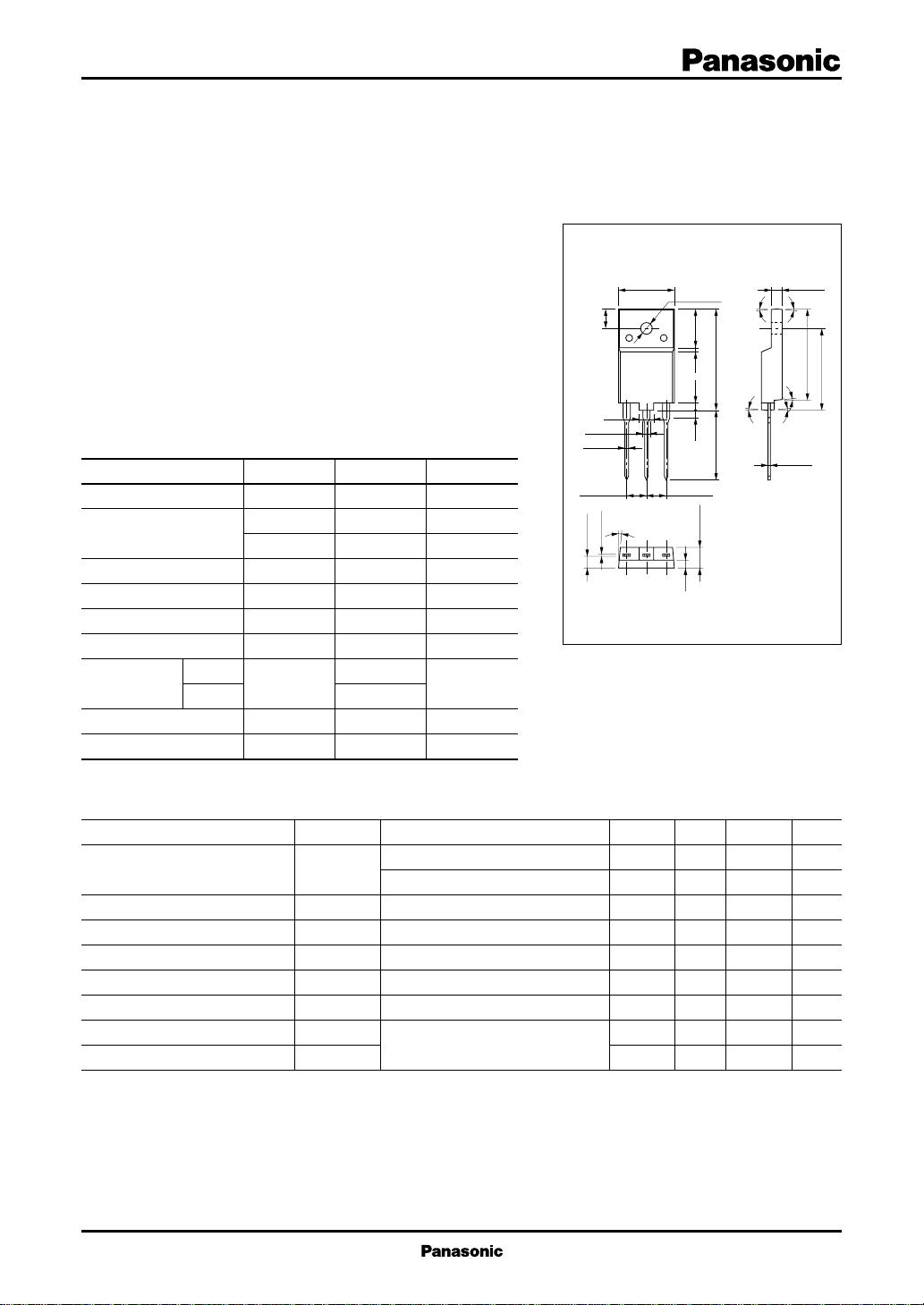
4.5
4.0
2.0±0.2
1.1±0.1
5.45±0.3
0.7±0.1
3.3±0.3
15.5±0.5
5°
123
φ3.2±0.1
5° 5°
26.5±0.5
5°
2.0 2.0 1.2 10.0
18.6±0.5
5.45±0.3
5.5±0.3
2.0
TOP–3E Full Pack Package
Unit: mm
3.0±0.3
23.4
5°
5°
0.7±0.1
1:Base
2:Collector
3:Emitter
22.0±0.5
Electrical Characteristics (T
■
Parameter
Collector cutoff current
Emitter cutoff current
Forward current transfer ratio
Collector to emitter saturation voltage
Base to emitter saturation voltage
Transition frequency
Storage time
Fall time
C
Symbol
I
CBO
I
EBO
h
FE
V
CE(sat)
V
BE(sat)
f
T
t
stg
t
f
=25˚C)
Conditions
VCB = 1000V, IE = 0
VCB = 1500V, IE = 0
VEB = 5V, IC = 0
VCE = 5V, IC = 10A
IC = 10A, IB = 2.5A
IC = 10A, IB = 2.5A
VCE = 10V, IC = 0.1A, f = 0.5MHz
IC = 10A, IB1 = 2.5A, IB2 = –5.0A
min
5
typ3max
50
1
50
10
3
1.5
2.7
0.2
Unit
µA
mA
µA
V
V
MHz
µs
µs
1
Po wer Transistors 2SC5516
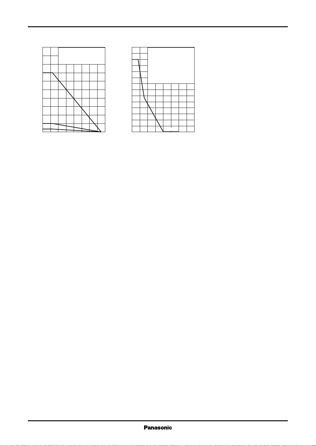
PC—Ta
100
)
90
W
(
80
C
70
60
50
40
30
20
10
Collector power dissipation P
0
0 16040 12080 14020 10060
(1) TC=Ta
(2) With a 100 × 100 × 2mm
Al heat sink
(3) Without heat sink
(1)
(2)
(3)
Ambient temperature Ta (˚C
Area of safe operation, horizontal operation ASO
35
30
)
A
(
25
C
20
15
10
Collector current I
5
0
0 2000500 15001000
)
Collector to emitter voltage VCE (V
f=64kHz, TC<90˚C
Area of safe operation with
respect to the single pulse
overload curve at the time of
switching ON, shutting down
by the high voltage spark,
holding down and like that,
during horizontal operation.
<1mA
)
2
 Loading...