

Panasonic 2SC5472 Datasheet
Transistors
2SC5472
Silicon NPN epitaxial planer type
For low-voltage low-noise high-frequency oscillation
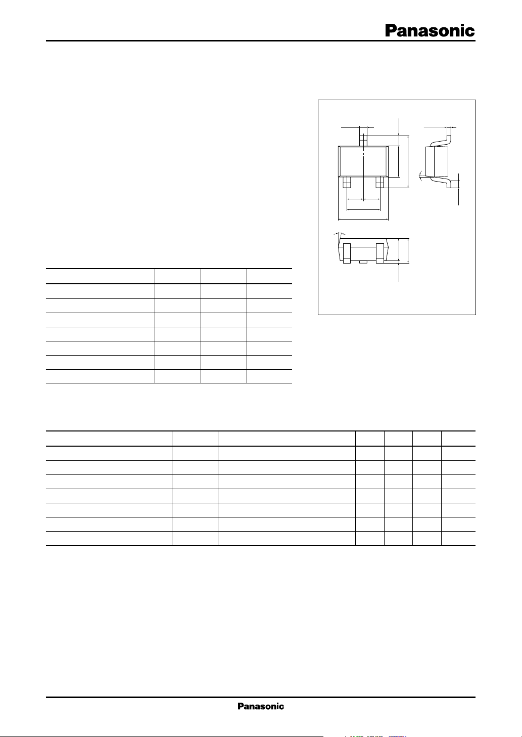
Unit: mm
+0.1
0.3
–0.0
(0.425)
0.15
+0.10
–0.05
■ Features
• High transition frequency f
• High gain of 8.2 dB and low noise of 1.8 dB at 3 V
• Optimum for RF amplification of a portable telephone and pager
• S-mini type package, allowing downsizing of the equipment and
automatic insertion through the tape packing and the magazine
packing.
T
■ Absolute Maximum Ratings Ta = 25°C
Parameter Symbol Rating Unit
Collector to base voltage V
Collector to emitter voltage V
Emitter to base voltage V
Collector current I
Collector power dissipation P
Junction temperature T
Storage temperature T
CBO
CEO
EBO
C
C
j
stg
9V
6V
1V
30 mA
150 mW
150 °C
−55 to +150 °C
132
(0.65)
(0.65)
1.3
±0.1
2.0
±0.2
10°
1: Base
2: Emitter EIAJ: SC-70
3: Collector S-Mini Type Package
Marking Symbol: 3A
±0.10
1.25
+0.2
±0.1
0.9
0.9
0 to 0.1
±0.1
2.1
5°
–0.1
■ Electrical Characteristics Ta = 25°C ± 3°C
Parameter Symbol Conditions Min Typ Max Unit
Collector cutoff current I
Emitter cutoff current I
CBO
EBO
Forward current transfer ratio h
Transition frequency f
Collector output capacitance C
Forward transfer gain | S
21e
Noise figure NF VCE = 3 V, IC = 3 mA, f = 1.5 GHz 1.8 3.0 dB
VCB = 9 V, IE = 01µA
VEB = 1 V, IC = 01µA
VCE = 3 V, IC = 10 mA 80 200
FE
VCE = 3 V, IC = 10 mA, f = 2 GHz 12.0 GHz
T
VCB = 3 V, IE = 0, f = 1 MHz 0.6 0.9 pF
ob
2
|
VCE = 3 V, IC = 10 mA, f = 2 GHz 6.0 8.0 dB
±0.1
0.2
1
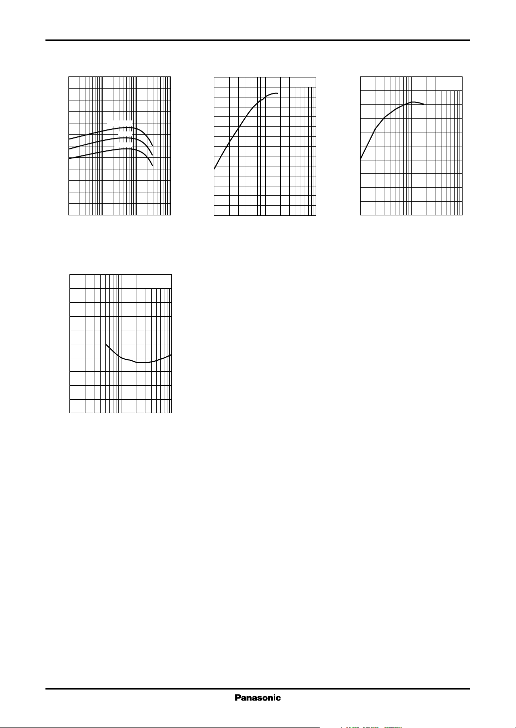
2SC5472 Transistors
| S
hFE I
240
200
FE
160
120
80
Forward current transfer ratio h
40
C
Ta = 75°C
25°C
−25°C
fT I
14
12
10
(GHz)
T
8
6
4
Transition frequency f
2
C
VCE = 3 V
(dB)
2
|
21e
Forward transfer gain | S
10
8
6
4
2
21e
| 2 I
C
VCE = 3 V
f = 2 GHz
0
0.1 0.3
1 3 10 30 100
Collector current IC (mA)
NF I
5
4
C
VCE = 3 V
f = 1.5 GHz
)
dB
(
3
2
Noise figure NF
1
0
0.1 0.3 1 3 10
Collector current IC (mA)
0
1 3 10 30 100
Collector current IC (mA)
0
1 3 10 30 100
Collector current IC (mA)
2
 Loading...