

Panasonic 2SC5243 Datasheet
Po wer Transistors
2SC5243
Silicon NPN triple diffusion mesa type
For horizontal deflection output
Features
■
●
High breakdown voltage, and high reliability through the use of a
glass passivation layer
●
High-speed switching
●
Wide area of safe operation (ASO)
Absolute Maximum Ratings (T
■
Parameter
Collector to base voltage
Collector to emitter voltage
Emitter to base voltage
Collector current
Peak collector current
Peak base current
Collector power
dissipation
TC=25°C
Ta=25°C
Junction temperature
Storage temperature
*
Non-repetitive peak
Symbol
V
V
V
I
C
I
CP
I
BP
P
C
T
j
T
stg
CBO
CES
EBO
*
=25˚C)
C
Ratings
1700
1700
6
15
30
10
200
3.5
150
–55 to +150
Unit
V
V
V
A
A
A
W
˚C
˚C
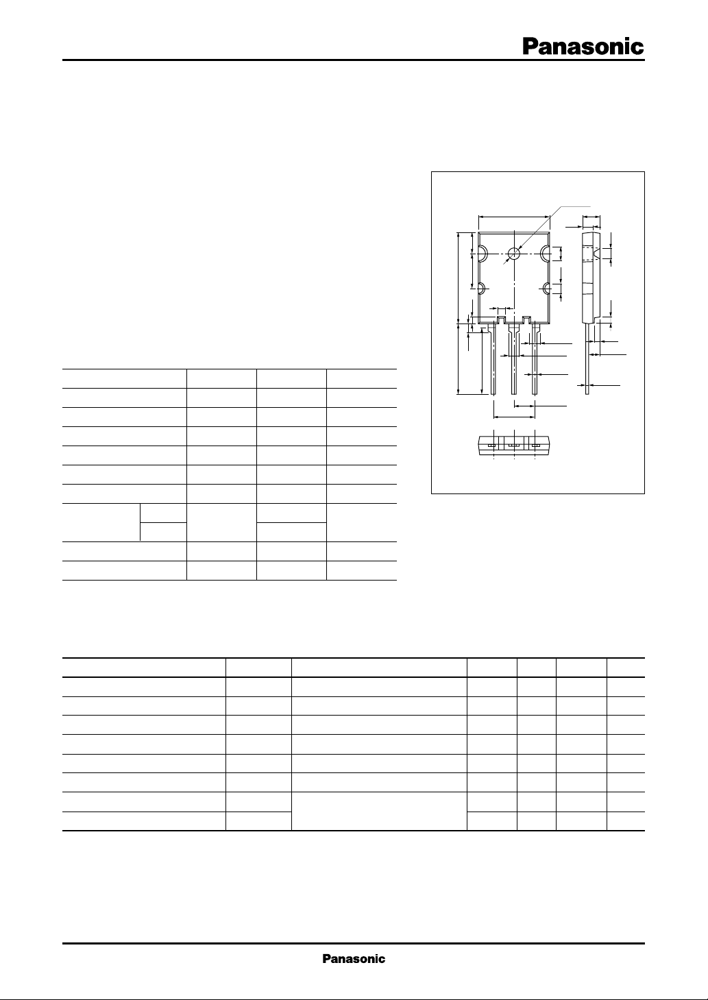
6.010.0
26.0±0.520.0±0.5
1.5
2.5
20.0±0.5
1.5
Solder Dip
10.9±0.5
123
φ 3.3±0.2
4.02.0
2.0±0.3
3.0±0.3
1.0±0.2
5.45±0.3
Unit: mm
5.0±0.3
3.0
3.0
2.0
1.5
2.7±0.3
0.6±0.2
1:Base
2:Collector
3:Emitter
TOP–3L Package
Electrical Characteristics (T
■
Parameter
Collector cutoff current
Emitter cutoff current
Forward current transfer ratio
Collector to emitter saturation voltage
Base to emitter saturation voltage
Transition frequency
Storage time
Fall time
C
Symbol
I
CBO
I
EBO
h
FE
V
CE(sat)
V
BE(sat)
f
T
t
stg
t
f
=25˚C)
Conditions
VCB = 1700V, IE = 0
VEB = 5V, IC = 0
VCE = 5V, IC = 10A
IC = 10A, IB = 2.8A
IC = 10A, IB = 2.8A
VCE = 10V, IC = 0.1A, f = 0.5MHz
IC = 12A, IB1 = 2.4A, IB2 = –4.8A,
Resistance loaded
min
5
typ
3
1.5
0.12
max
1
50
12
3
1.5
2.5
0.2
Unit
µA
µA
V
V
MHz
µs
µs
1
Po wer Transistors 2SC5243
PC—Ta IC—V
240
220
)
W
(
200
C
180
160
140
120
100
80
60
40
Collector power dissipation P
20
0
0 16040 12080 14020 10060
Ambient temperature Ta (˚C
)
100
V
(
30
CE(sat)
10
3
1
0.3
TC=–25˚C
0.1
0.03
0.01
Collector to emitter saturation voltage V
0.1 1 10 1000.3 3 30
(1) TC=Ta
(2) With a 100 × 100 × 2mm
Al heat sink
(3) Without heat sink
(1)
=3.0W)
(P
C
(3)
(2)
V
CE(sat)—IC
IC/IB=3.5
25˚C
100˚C
Collector current IC (A
)
)
CE
16
14
)
12
A
(
C
10
8
6
4
Collector current I
2
0
012108264
TC=25˚C
IB=1000mA
800mA
600mA
400mA
200mA
Collector to emitter voltage VCE (V
V
BE(sat)—IC
100
)
V
(
BE(sat)
10
TC=–25˚C
1
100˚C
25˚C
0.1
Base to emitter saturation voltage V
0.01
0.1 1 10 100
Collector current IC (A
IC/IB=3.5
)
hFE—I
1000
FE
100
10
1
Forward current transfer ratio h
0.1
0.01 0.1 1 10
)
Collector current IC (A
Area of safe operation, horizontal operation ASO
50
40
)
A
(
C
30
20
Collector current I
10
0
0 20001600400 1200800
Collector to emitter voltage VCE (V
C
=5V
V
CE
TC=100˚C
25˚C
–25˚C
)
f=64kHz, TC=25˚C
Area of safe operation for
the single pulse load curve
due to discharge in the
high-voltage rectifier tube
during horizontal operation
<1mA
)
1000
)
100
˚C/W
(
(t)
th
10
1
0.1
Thermal resistance R
0.01
–4
10
–3
2
R
—t
th(t)
Note: Rth was measured at Ta=25˚C and under natural convection
(1) P
=10V × 0.3A (3W) and without heat sink
T
=10V × 1.0A (10W) and with a 100 × 100 × 2mm Al heat sink
(2) P
T
(1)
(2)
–1
–2
10
10
Time t (s
1010
110
)
2
10
3
4
10
 Loading...