

Panasonic 2SC5216 Datasheet
Transistor
2.8
+0.2
–0.3
1.5
+0.25
–0.050.65±0.15 0.65±0.15
3
1
2
0.950.95
1.9±0.2
0.4
+0.1
–0.05
1.1
+0.2
–0.1
0.8
0.4±0.2
0 to 0.1
0.16
+0.1
–0.06
1.45
0.1 to 0.3
2.9
+0.2
–0.05
2SC5216
Silicon NPN epitaxial planer type
For high-frequency amplification/oscillation/mixing
Features
■
●
High transition frequency fT.
●
Mini type package, allowing downsizing of the equipment and
automatic insertion through the tape packing and the magazine
packing.
Absolute Maximum Ratings (Ta=25˚C)
■
Parameter
Collector to base voltage
Collector to emitter voltage
Emitter to base voltage
Collector current
Collector power dissipation
Junction temperature
Storage temperature
Symbol
V
CBO
V
CEO
V
EBO
I
C
P
C
T
j
T
stg
Ratings
15
8
3
50
200
150
–55 ~ +150
Unit
mA
mW
˚C
˚C
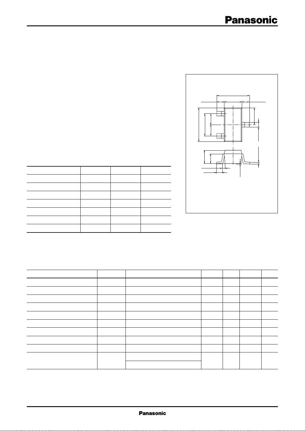
Unit: mm
V
V
V
1:Base JEDEC:TO–236
2:Emitter EIAJ:SC–59
3:Collector Mini T ype Package
Marking symbol : FB
Electrical Characteristics (Ta=25˚C)
■
Parameter
Emitter cutoff current
Collector to base voltage
Forward current transfer ratio
Collector to emitter saturation voltage
Base to emitter voltage
Transition frequency
Collector output capacitance
Common emitter reverse transfer capacitance
Power gain
hFE ratio
Symbol
I
EBO
V
CBO
h
FE
V
CE(sat)
V
BE
f
T
C
ob
C
rb
PG
h
FE(RATIO)
Conditions
VEB = 2V, IC = 0
IC = 100µA, IE = 0
VCE = 4V, IC = 2mA
IC = 20mA, IB = 4mA
VCE = 4V, IC = 2mA
VCB = 10V, IE = –15mA, f = 200MHz
VCB = 10V, IE = 0, f = 1MHz
VCB = 6V, IE = 0, f = 1MHz
VCB = 10V, IE = –10mA, f = 200MHz
VCE = 4V, IC = 100µA
VCE = 4V, IC = 2mA
min
15
100
0.8
0.6
14
0.6
typ
0.7
1.3
1.0
0.4
18
max
2
350
0.5
1.9
1.4
22
1.5
Unit
µA
V
V
V
GHz
pF
pF
dB
1
Transistor
2SC5216
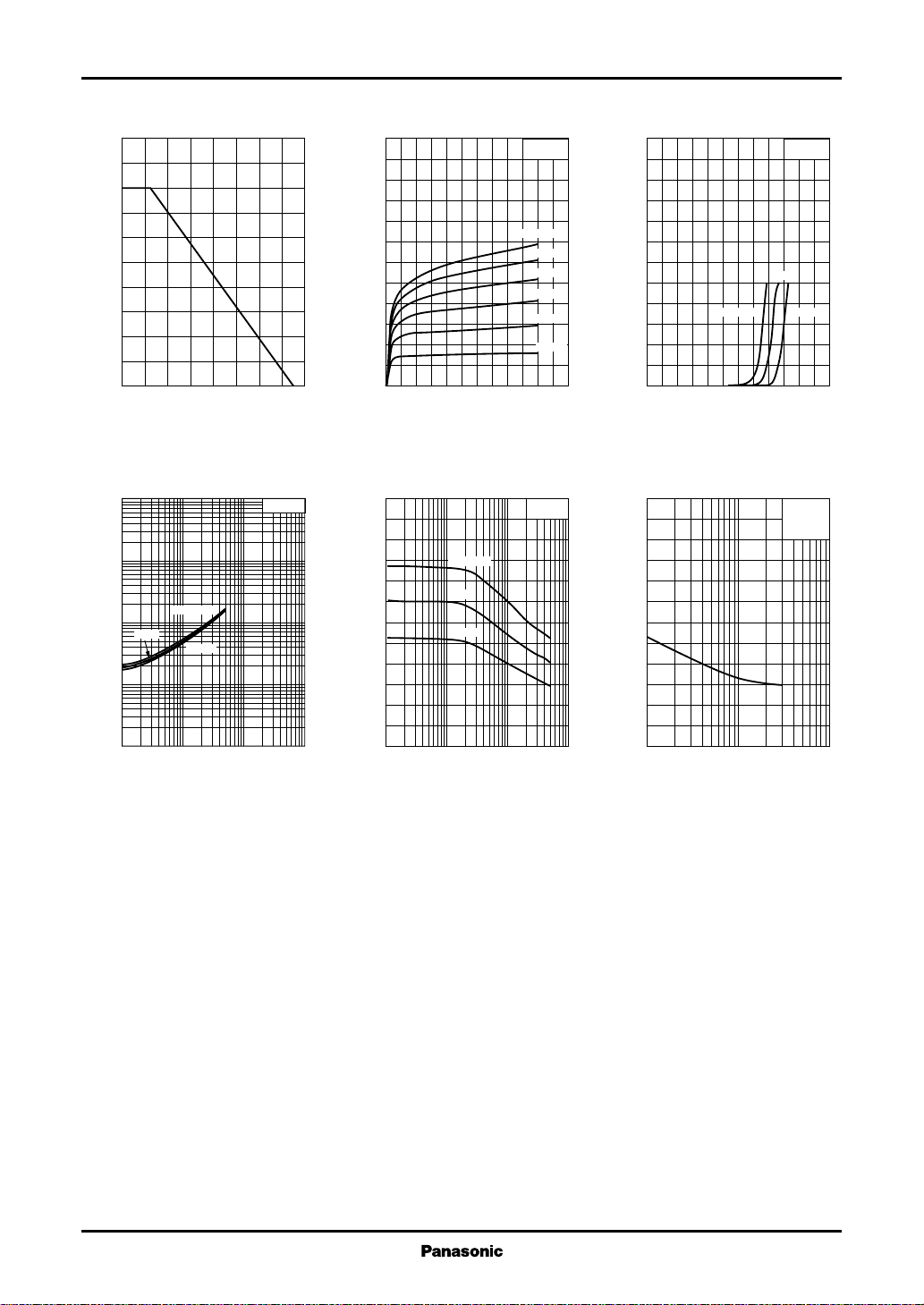
PC — Ta IC — V
250
)
mW
(
200
C
150
100
50
Collector power dissipation P
0
0 16040 12080 14020 10060
Ambient temperature Ta (˚C
V
— I
CE(sat)
)
10
V
(
3
CE(sat)
1
0.3
0.1
0.03
0.01
0.003
0.001
Collector to emitter saturation voltage V
1 10 100 10003 30 300
Ta=75˚C
25˚C
–25˚C
Collector current IC (mA
)
C
IC/IB=5
)
CE
120
100
)
mA
(
80
C
60
40
Collector current I
20
0
0654132
IB=600µA
Collector to emitter voltage VCE (V
hFE — I
C
300
FE
250
Ta=75˚C
200
150
100
50
Forward current transfer ratio h
0
0.1 1 10 1000.3 3 30
25˚C
–25˚C
Collector current IC (mA
Ta=25˚C
500µA
400µA
300µA
200µA
100µA
VCE=4V
)
IC — V
120
100
)
mA
(
80
C
60
40
Collector current I
20
0
01.21.00.80.2 0.60.4
)
Base to emitter voltage VBE (V
Cob — V
3.0
)
pF
(
2.5
ob
2.0
1.5
1.0
0.5
Collector output capacitance C
0
1 3 10 30 100
Collector to base voltage VCB (V
BE
VCE=4V
25˚C
Ta=75˚C –25˚C
CB
f=1MHz
I
=0
E
Ta=25˚C
)
)
2
 Loading...