

Panasonic 2SC5018 Datasheet
Transistor
2SC5018
Silicon NPN triple diffusion planer type
For high breakdown voltage high-speed switching
Features
■
●
High collector to base voltage V
●
High emitter to base voltage V
Absolute Maximum Ratings (Ta=25˚C)
■
Parameter
Collector to base voltage
Collector to emitter voltage
Emitter to base voltage
Peak collector current
Collector current
Collector power dissipation
Junction temperature
Storage temperature
*
Printed circuit board: Copper foil area of 1cm2 or more, and the board
thickness of 1.7mm for the collector portion
Symbol
V
V
V
I
CP
I
C
P
C
T
j
T
stg
CBO
CEO
EBO
*
EBO
CBO
.
.
Ratings
500
400
7
1.5
0.8
1
150
–55 ~ +150
Unit
V
V
V
A
A
W
˚C
˚C
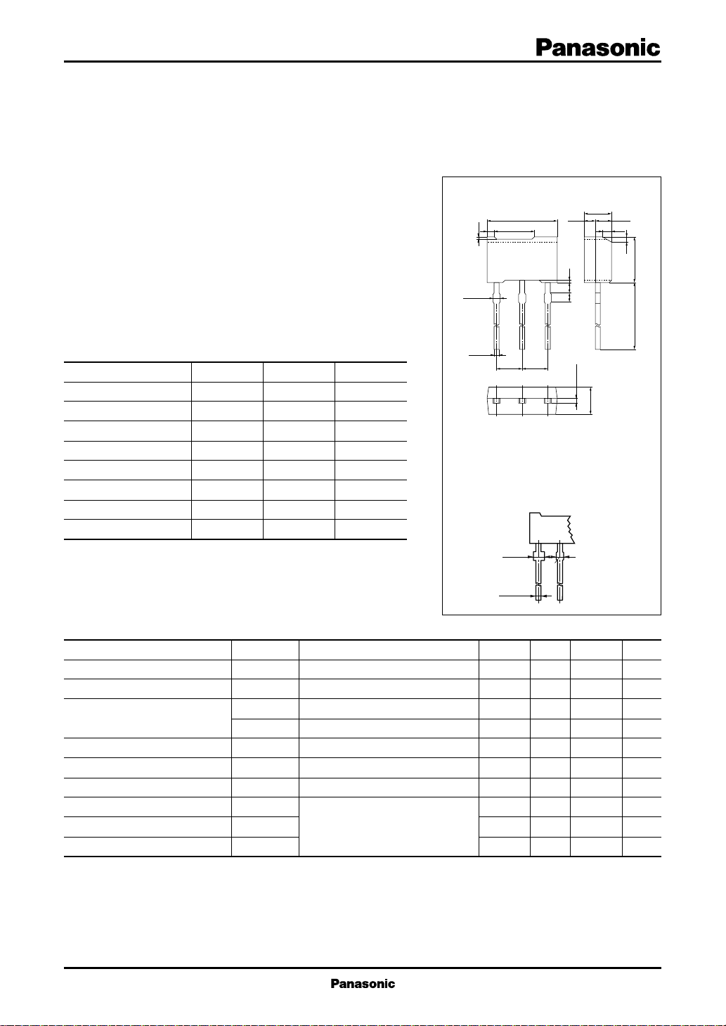
6.9±0.1
4.00.7 0.8
0.15
0.65 max.
+0.1
0.45
–0.05
2.5±0.5 2.5±0.5
Note: In addition to the
lead type shown in
the upper figure, the
type as shown in
the lower figure is
also available.
1.2±0.1
+
0.1
0.45
–
0.05
1.05
±0.05 (1.45)
0.21.01.0
–0.05
+0.1
321
0.45
1:Emitter
2:Collector
3:Base
MT2 Type Package
0.65
max.
Unit: mm
2.5±0.1
0.5
4.5±0.114.5±0.5
2.5±0.1
(HW type)
Electrical Characteristics (Ta=25˚C)
■
Parameter
Collector cutoff current
Emitter cutoff current
Forward current transfer ratio
Collector to emitter saturation voltage
Base to emitter saturation voltage
Transition frequency
Turn-on time
Storage time
Fill time
Symbol
I
CBO
I
EBO
h
FE1
h
FE2
V
CE(sat)
V
BE(sat)
f
T
t
on
t
stg
t
f
Conditions
VCB = 500V, IE = 0
VEB = 7V, IC = 0
VCE = 5V, IC = 10mA
VCE = 5V, IC = 300mA
IC = 100mA, IB = 10mA
IC = 100mA, IB = 10mA
*1
*1
*1
VCB = 10V, IE = –50mA, f = 10MHz
IC = 200mA, IB1 = 40mA
IB2 = –40mA, VCC = 150V
min
50
10
typ
max
100
100
300
0.1
0.8
0.5
1.0
20
0.7
4.0
0.4
*1
Pulse measurement
Unit
µA
µA
V
V
MHz
µs
µs
µs
1
Transistor 2SC5018
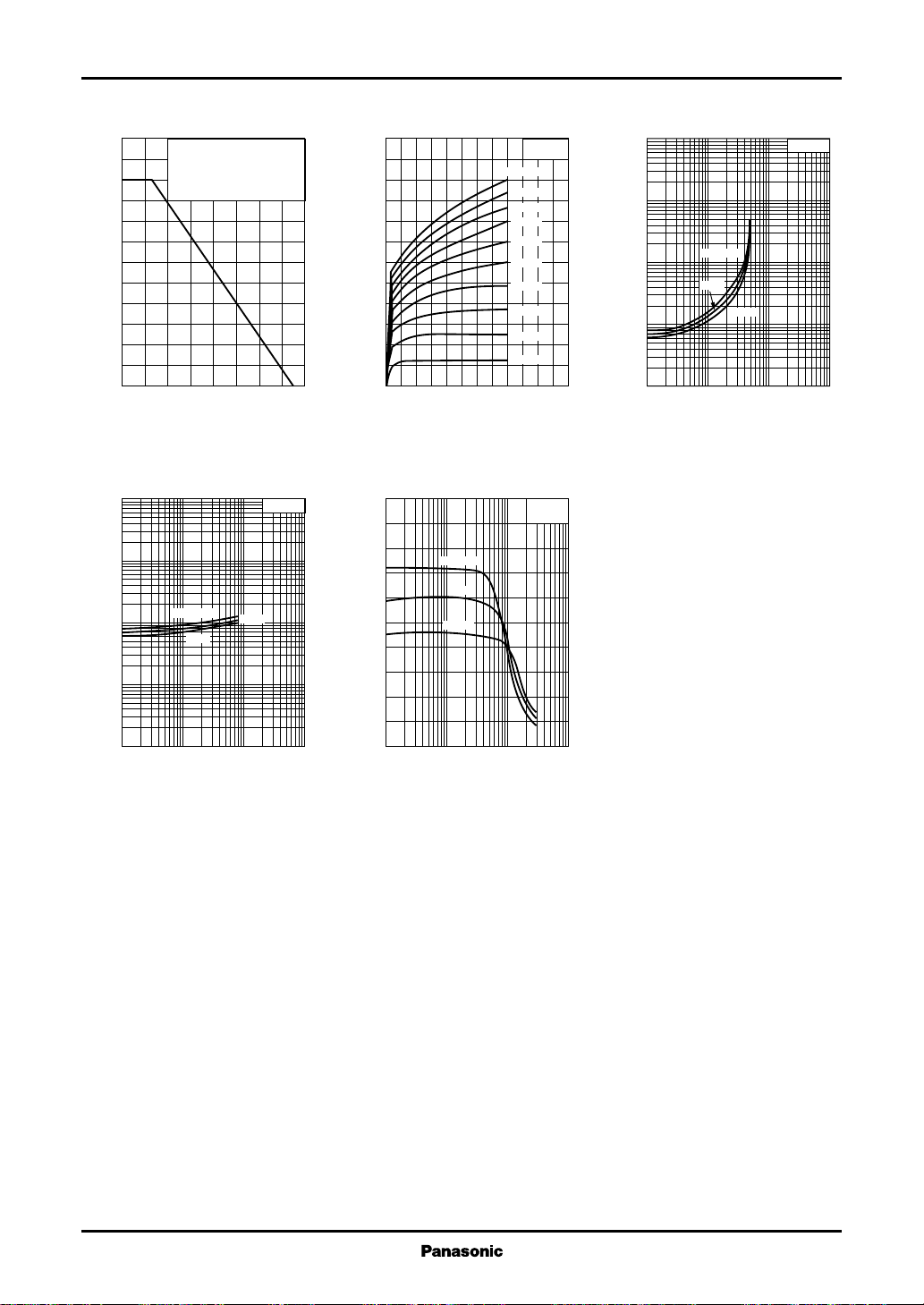
PC — Ta IC — V
1.2
)
W
(
1.0
C
0.8
0.6
0.4
0.2
Collector power dissipation P
0
100
)
V
(
30
BE(sat)
10
3
1
0.3
0.1
0.03
Base to emitter saturation voltage V
0.01
0.01 0.1 1 100.03 0.3 3
Printed circut board: Copper
foil area of 1cm
the board thickness of 1.7mm
for the collector portion.
0 16040 12080 14020 10060
2
or more, and
Ambient temperature Ta (˚C
V
— I
BE(sat)
Ta=–25˚C
75˚C
C
IC/IB=10
25˚C
Collector current IC (A
)
V
CE
120
100
)
mA
(
80
C
60
40
Collector current I
20
0
012108264
)
Collector to emitter voltage VCE (V
hFE — I
200
FE
160
120
80
40
Ta=75˚C
25˚C
–25˚C
Ta=25˚C
IB=1.0mA
0.9mA
0.8mA
0.7mA
0.6mA
0.5mA
0.4mA
0.3mA
0.2mA
0.1mA
C
VCE=5V
)
100
V
(
30
CE(sat)
10
3
1
0.3
0.1
0.03
0.01
Collector to emitter saturation voltage V
0.01 0.1 1 100.03 0.3 3
)
Collector current IC (A
CE(sat)
Ta=75˚C
25˚C
— I
–25˚C
C
IC/IB=10
)
Forward current transfer ratio h
0
0.001 0.01 0.1 10.003 0.03 0.3
Collector current IC (A
)
2
 Loading...