

Panasonic 2SC4835G User Manual
This product complies with the RoHS Directive (EU 2002/95/EC).
Transistors
2SC4835G
Silicon NPN epitaxial planar type
For UHF band low-noise amplification
■ Features
• Low noise figure NF
• High forward transfer gain S
• High transition frequency f
• S-Mini type package, allowing downsizing of the equipment
and automatic insertion through the tape packing and the magazine packing
2
21e
T
■ Package
•
Code
SMini3-F2
•
Marking Symbol: 3M
•
Pin Name
1: Base
2: Emitter
3: Collector
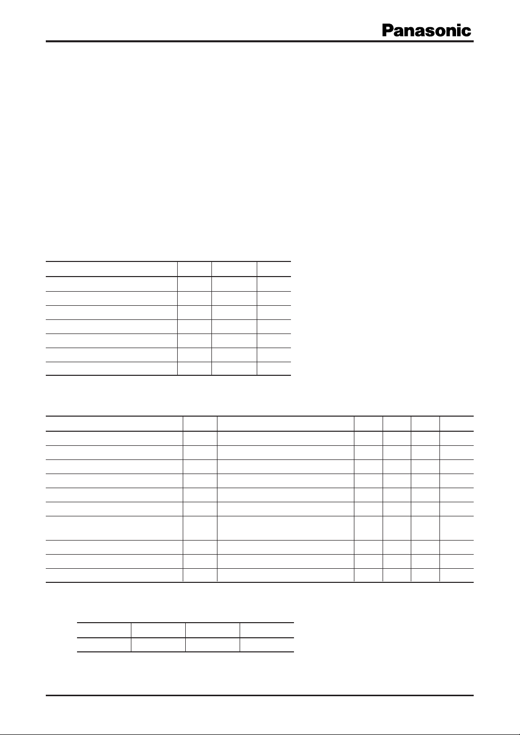
■ Absolute Maximum Ratings Ta = 25°C
Parameter Symbol Rating Unit
Collector-base voltage (Emitter open) V
Collector-emitter voltage (Base open) V
Emitter-base voltage (Collector open) V
Collector current I
Collector power dissipation P
Junction temperature T
Storage temperature T
CBO
CEO
EBO
C
C
j
stg
15 V
10 V
2V
80 mA
150 mW
150 °C
−55 to +150 °C
■ Electrical Characteristics Ta = 25°C ± 3°C
Parameter Symbol Conditions Min Typ Max Unit
Collector-base voltage (Emitter open) V
Collector-emitter voltage (Base open) V
Collector-base cutoff current (Emitter open)
Emitter-base cutoff current (Collector open)
1, 2
Forward current transfer ratio
Transition frequency f
Collector output capacitance C
(Common base, input open circuited)
Forward transfer gain S
Maximum unilateral power gain G
Noise figure NF VCE = 8 V, IC = 7 mA, f = 800 MHz 1.3 2.0 dB
Note) 1. Measuring methods are based on JAPANESE INDUSTRIAL STANDARD JIS C 7030 measuring methods for transistors.
2.*1: Pulse measurement
2: Rank classification
*
Rank Q R S
h
FE
*
50 to 100 80 to 130 100 to 200
CBOIC
CEOIC
I
CBO
I
EBO
h
FE
21e
UM
= 10 µA, IE = 015V
= 100 µA, IB = 010 V
VCB = 10 V, IE = 01µA
VEB = 2 V, IC = 01µA
VCE = 8 V, IC = 20 mA 50 200
VCE = 8 V, IC = 15 mA, f = 800 MHz 5 6 GHz
T
VCB = 10 V, IE = 0, f = 1 MHz 0.7 1.2 pF
ob
2VCE = 8 V, IC = 15 mA, f = 800 MHz 11 14 dB
VCE = 8 V, IC = 15 mA, f = 800 MHz 15 dB
Publication date: May 2007 SJC00368AED
1
2SC4835G
This product complies with the RoHS Directive (EU 2002/95/EC).
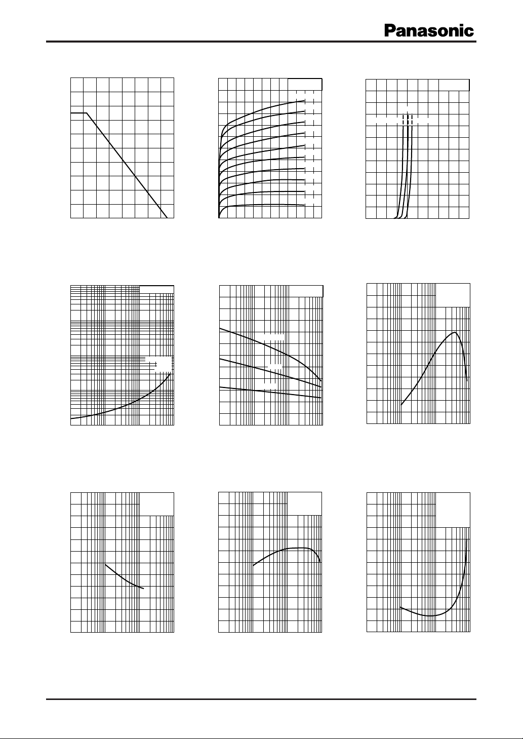
PC T
200
)
mW
160
(
C
120
80
40
Collector power dissipation P
0
0 16040 12080
Ambient temperature Ta (°C
V
I
)
V
(
CE(sat)
100
10
1
0.1
CE(sat)
a
C
IC / IB = 10
Ta = 75°C
25°C
−25°C
IC V
hFE I
Ta = 75°C
25°C
−25°C
CE
IB = 200 µA
C
Ta = 25°C
180 µA
160 µA
140 µA
120 µA
100 µA
80 µA
60 µA
40 µA
20 µA
VCE = 8 V
120
100
)
mA
(
80
C
60
40
Collector current I
20
0
02.01.60.4 1.20.8
)
12
10
)
GHz
(
8
T
6
4
Transition frequency f
2
24
20
)
mA
(
16
C
12
8
Collector current I
4
0
012108264
)
Collector-emitter voltage VCE (V
600
500
FE
400
300
200
Forward current transfer ratio h
100
IC V
BE
VCE = 8 V
25°C
Ta = 75°C
−25°C
Base-emitter voltage VBE (V
fT I
C
VCE = 8 V
f = 800 MHz
= 25°C
T
a
)
Collector-emitter saturation voltage V
0.01
0.1 1 10 100
Collector current IC (mA
Cob V
2.4
(pF)
ob
C
2.0
1.6
1.2
0.8
0.4
Collector output capacitance
(Common base, input open circuited)
0
0.1 1 10 100
CB
Collector-base voltage VCB (V
2
)
IE = 0
f = 1 MHz
= 25°C
T
a
0
0.1 1 10 100
Collector current IC (mA
GUM I
24
)
dB
(
20
UM
C
)
VCE = 8 V
f = 800 MHz
= 25°C
T
a
0
0.1 1 10 100
C
VCE = 8 V
= 50 Ω)
(R
g
f = 800 MHz
= 25°C
T
a
)
Collector current IC (mA
NF I
12
10
)
16
12
8
4
dB
8
(
6
4
Noise figure NF
2
Maximum unilateral power gain G
0
0.1 1 10 100
)
Collector current IC (mA
)
0
0.1 1 10 100
Collector current IC (mA
)
SJC00368AED
 Loading...