

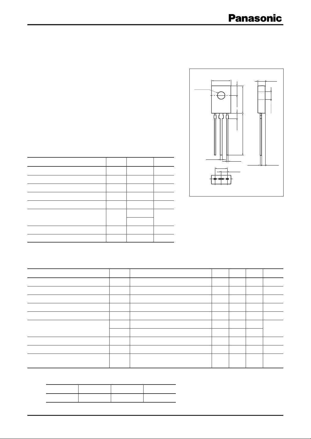
Panasonic 2SC1846 Diagram
Power Transistors
2SC1846
Silicon NPN epitaxial planar type
For medium output power amplification
Complementary to 2SA0885
■ Features
• Low collector-emitter saturation voltage V
• Output of 3 W can be obtained by a complementary pair with
2SA0885
• TO-126B package which requires no insulation plate for installation to the heat sink
CE(sat)
■ Absolute Maximum Ratings Ta = 25°C
Parameter Symbol Rating Unit
Collector-base voltage (Emitter open) V
Collector-emitter voltage (Base open) V
Emitter-base voltage (Collector open) V
Collector current I
Peak collector current I
Collector power dissipation P
CBO
CEO
EBO
C
CP
C
Junction temperature T
Storage temperature T
stg
Note)*: With a 100 × 100 × 2 mm Al heat sink
j
45 V
35 V
5V
1A
1.5 A
1.2 W
*
5.0
150 °C
−55 to +150 °C
φ 3.16
±0.1
0.75
+0.5
8.0
–0.1
±0.1
4.6
±0.2
123
±0.5
±0.3
11.0
3.8
±0.1
1.9
±1.0
16.0
0.5
±0.1
0.5
2.3
±0.2
TO-126B-A1 Package
±0.1
1: Emitter
2: Collector
3: Base
Unit: mm
3.2
±0.2
±0.1
3.05
1.76
±0.1
■ Electrical Characteristics Ta = 25°C ± 3°C
Parameter Symbol Conditions Min Typ Max Unit
Collector-base voltage (Emitter open) V
Collector-emitter voltage (Base open) V
Collector-base cutoff current (Emitter open)
Collector-emitter cutoff current (Base open)
Emitter-base cutoff current (Collector open)
Forward current transfer ratio h
Collector-emitter saturation voltage V
CBOIC
CEOIC
I
CBO
I
CEO
I
EBO
FE1
h
FE2
CE(sat)IC
Transition frequency f
Collector output capacitance C
(Common base, input open circuited)
Note) 1. Measuring methods are based on JAPANESE INDUSTRIAL STANDARD JIS C 7030 measuring methods for transistors.
2.*: Rank classification
Rank Q R S
h
FE1
Publication date: February 2003 SJD00094BED
85 to 170 120 to 240 170 to 340
= 1 mA, IE = 045V
= 2 mA, IB = 035V
VCB = 20 V, IE = 0 0.1 µA
VCE = 20 V, IB = 0 100 µA
VEB = 5 V, IC = 010µA
*
VCE = 10 V, IC = 500 mA 85 340
VCE = 5 V, IC = 1 A 50
= 500 mA, IB = 50 mA 0.5 V
VCB = 10 V, IE = −50 mA, f = 200 MHz 200 MHz
T
VCB = 10 V, IE = 0, f = 1 MHz 20 pF
ob
1
2SC1846
6
)
5
W
(
C
4
3
2
1
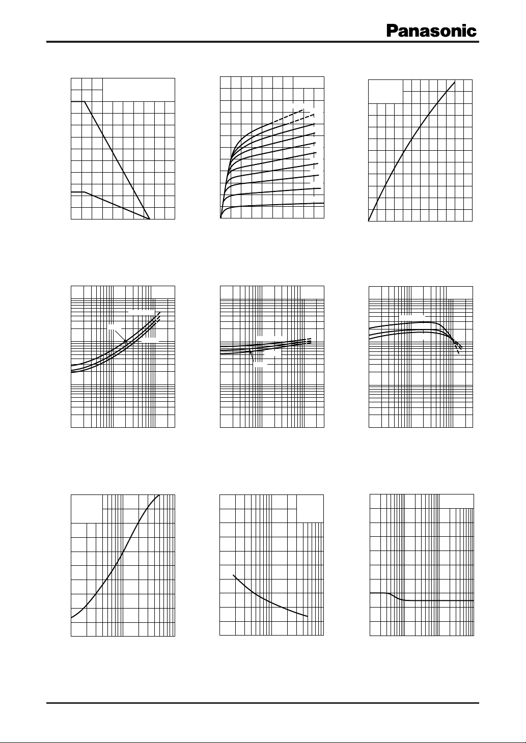
Collector power dissipation P
0
0 20040 80 160120
)
V
(
1
CE(sat)
0.1
(1)With a 100×100×2mm
Al heat sink
(2)Without heat sink
(1)
(2)
Ambient temperature Ta (°C
V
I
CE(sat)
TC=100˚C
25˚C
PC T
a
1.50
1.25
)
A
(
1.00
C
0.75
0.50
Collector current I
0.25
0
01024 86
)
C
IC/IB=10
–25˚C
Collector-emitter voltage VCE (V
)
10
V
(
BE(sat)
1
IC V
V
BE(sat)
TC=–25˚C
25˚C
100˚C
CE
I
TC=25˚C
IB=10mA
C
9mA
8mA
7mA
6mA
5mA
4mA
3mA
2mA
1mA
IC/IB=10
1.2
VCE=10V
Ta=25˚C
1.0
)
A
(
0.8
C
0.6
0.4
Collector current I
0.2
0
)
012210486
1000
FE
100
IC I
B
Base current IB (mA
hFE I
C
TC=100˚C
25˚C
–25˚C
)
VCE=10V
0.01
Collector-emitter saturation voltage V
0.001
0.01
0.1 1
Collector current IC (A
fT I
200
VCB=10V
f=200MHz
T
=25˚C
C
)
160
MHz
(
T
120
80
40
Transition frequency f
0
−1 −10 −100
E
Emitter current IE (mA
0.1
10
Forward current transfer ratio h
Base-emitter saturation voltage V
0.01
0.01 10.1
)
Collector current IC (A
Cob V
50
(pF)
ob
C
40
30
20
10
Collector output capacitance
(Common base, input open circuited)
0
1 10 100
)
Collector-base voltage VCB (V
CB
)
IE=0
f=1MHz
T
=25˚C
C
)
1
0.01 10.1
Collector current IC (A
V
R
100
(V)
80
CER
V
60
40
20
Collector-emitter voltage
(Resistor between B and E)
0
0.1 1 10 100
CER
Base-emitter resistance RBE (kΩ
BE
)
IC=10mA
T
=25˚C
C
)
2
SJD00094BED
 Loading...