

Panasonic 2SC1360A, 2SC1360 Datasheet
Transistor
5.9±0.2
2.54±0.15
0.7±0.1
4.9±0.2
8.6±0.2
0.7
+0.3
–0.2
13.5±0.53.2
0.45
+0.2
–0.1
1.271.27
0.45
+0.2
–0.1
132
2SC1360, 2SC1360A
Silicon NPN epitaxial planer type
For intermadiate frequency amplification of TV image
Features
■
●
High transition frequency fT.
●
Large collector power dissipation PC.
Absolute Maximum Ratings (Ta=25˚C)
■
Parameter
Collector to
base voltage
Collector to
emitter voltage
2SC1360
2SC1360A
2SC1360
2SC1360A
Emitter to base voltage
Collector current
Collector power dissipation
Junction temperature
Storage temperature
Electrical Characteristics (Ta=25˚C)
■
Parameter
Collector cutoff current
Collector to base
voltage
Collector to emitter
voltage
Emitter to base voltage
Forward current transfer ratio
Collector to emitter saturation voltage
Transition frequency
Common emitter reverse transfer capacitance
Power gain
Symbol
2SC1360
2SC1360A
2SC1360
2SC1360A
Ratings
V
CBO
V
CEO
V
EBO
I
C
P
C
T
j
T
stg
50
60
45
60
4
50
1
150
–55 ~ +150
Symbol
I
V
V
V
h
V
f
C
PG
CBO
FE
T
CBO
CEO
EBO
CE(sat)
re
VCB = 20V, IE = 0
IC = 100µA, IE = 0
IC = 1mA, IB = 0
IE = 100µA, IC = 0
VCB = 10V, IE = –10mA
IC = 20mA, IB = 2mA
VCB = 10V, IE = –10mA, f = 100MHz
VCE = 10V, IC = 1mA, f = 10.7MHz
VCB = 10V, IE = –10mA, f = 58MHz
Unit
V
V
V
mA
W
˚C
˚C
Conditions
min
50
60
45
60
4
20
300
22
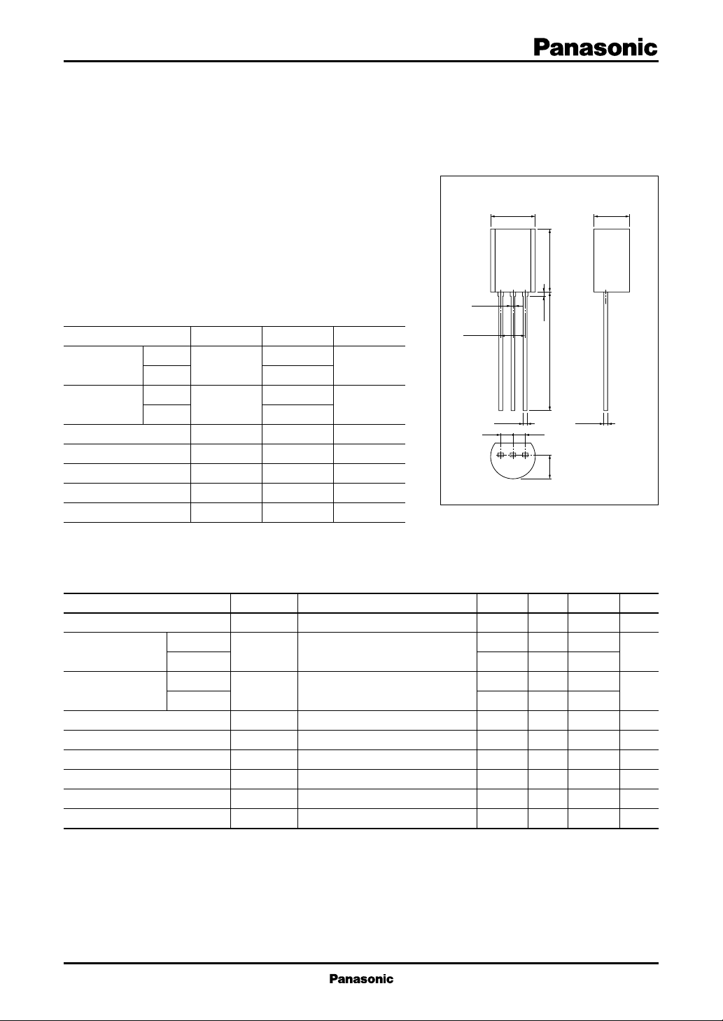
1:Emitter
2:Collector
3:Base
EIAJ:SC–51
TO–92L Package
typ max
100
100
0.4
1.5
30
Unit: mm
Unit
nA
V
V
V
V
MHz
pF
dB
1
Transistor
2SC1360, 2SC1360A
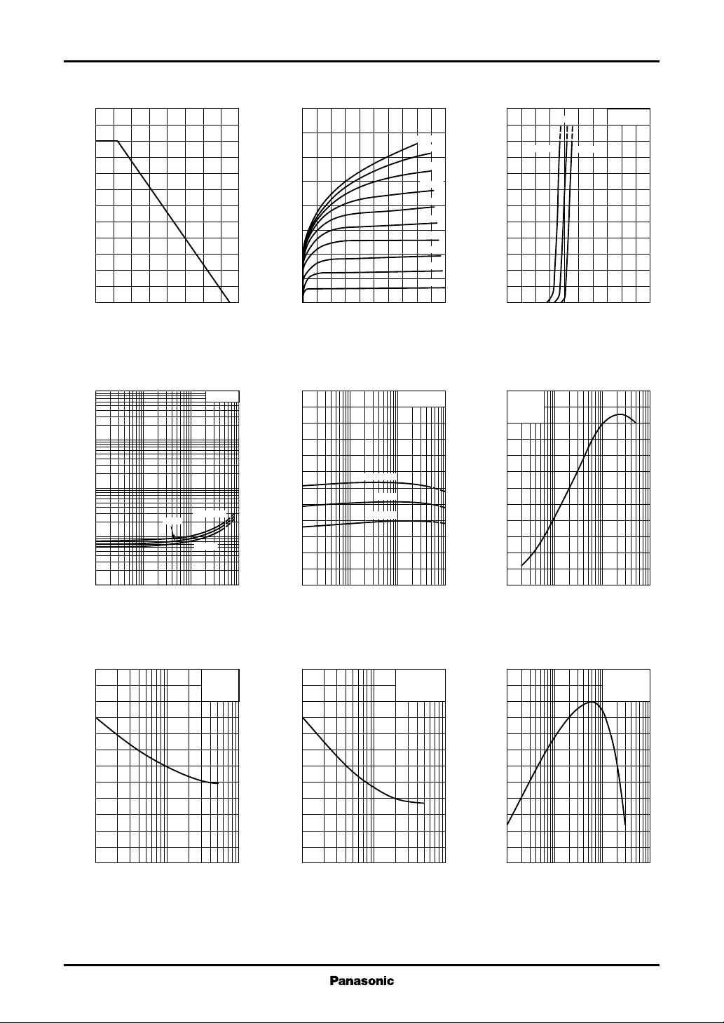
PC — Ta IC — V
1.2
)
W
(
1.0
C
0.8
0.6
0.4
0.2
Collector power dissipation P
0
0 16040 12080 14020 10060
Ambient temperature Ta (˚C
V
— I
CE(sat)
)
100
V
(
30
CE(sat)
10
3
1
0.3
0.1
0.03
0.01
Collector to emitter saturation voltage V
0.1 1 10 1000.3 3 30
25˚C
Collector current IC (mA
)
C
IC/IB=10
Ta=75˚C
–25˚C
)
CE
80
70
)
60
mA
(
C
50
40
30
20
Collector current I
10
0
0108264
IB=2.0mA
Collector to emitter voltage VCE (V
hFE — I
C
120
FE
100
80
60
40
20
Forward current transfer ratio h
0
0.1 1 10 1000.3 3 30
VCE=10V
Ta=75˚C
25˚C
–25˚C
Collector current IC (mA
1.8mA
1.6mA
1.4mA
1.2mA
1.0mA
0.8mA
0.6mA
0.4mA
0.2mA
)
60
50
)
mA
(
40
C
30
20
Collector current I
10
0
02.01.60.4 1.20.8
)
Base to emitter voltage VBE (V
600
)
500
MHz
(
T
400
300
200
100
Transition frequency f
0
– 0.1 –1 –10 –100– 0.3 –3 –30
IC — V
BE
25˚C
Ta=75˚C
VCB=10V
Ta=25˚C
–25˚C
fT — I
E
Emitter current IE (mA
VCE=10V
)
)
)
pF
(
Cob — V
3.0
2.5
ob
2.0
1.5
1.0
0.5
CB
Collector output capacitance C
0
1 3 10 30 100
Collector to base voltage VCB (V
2
IE=0
f=1MHz
Ta=25˚C
Cre — V
)
–2.4
pF
(
re
–2.0
–1.6
–1.2
– 0.8
– 0.4
Common emitter reverse transfer capacitance C
0
1 3 10 30 100
)
Collector to emitter voltage VCE (V
CE
IC=1mA
f=10.7MHz
Ta=25˚C
)
dB
(
Power gain PG
)
PG — I
E
30
25
20
15
10
5
0
– 0.1 –1 –10 –100– 0.3 –3 –30
VCB=10V
f=58MHz
Ta=25˚C
Emitter current IE (mA
)
 Loading...