

Panasonic 2SB1605 Datasheet
Po wer Transistors
2SB1605, 2SB1605A
Silicon PNP epitaxial planar type
For low-freauency power amplification
Features
■
●
High forward current transfer ratio hFE which has satisfactory linearity
●
Low collector to emitter saturation voltage V
●
Full-pack package with outstanding insulation, which can be in-
CE(sat)
stalled to the heat sink with one screw
Absolute Maximum Ratings (T
■
Parameter
Collector to
base voltage
Collector to
emitter voltage
2SB1605
2SB1605A
2SB1605
2SB1605A
Emitter to base voltage
Peak collector current
Collector current
Collector power
dissipation
TC=25°C
Ta=25°C
Junction temperature
Storage temperature
Electrical Characteristics (T
■
Symbol
V
V
V
I
CP
I
C
P
C
T
j
T
stg
Parameter
Collector cutoff
current
Collector cutoff
current
2SB1605
2SB1605A
2SB1605
2SB1605A
Emitter cutoff current
Collector to emitter
voltage
2SB1605
2SB1605A
Forward current transfer ratio
Base to emitter voltage
Collector to emitter saturation voltage
Transition frequency
Turn-on time
Storage time
Fall time
*
h
Rank classification
FE1
Rank Q P
h
FE1
70 to 150 120 to 250
CBO
CEO
EBO
C
Symbol
I
CES
I
CEO
I
EBO
V
CEO
*
h
FE1
h
FE2
V
BE
V
CE(sat)
f
T
t
on
t
stg
t
f
=25˚C)
C
Ratings
–60
–80
–60
–80
–5
–5
–3
35
2
150
–55 to +150
=25˚C)
VCE = –60V, VBE = 0
VCE = –80V, VBE = 0
VCE = –30V, IB = 0
VCE = –60V, IB = 0
VEB = –5V, IC = 0
IC = –30mA, IB = 0
VCE = –4V, IC = –1A
VCE = –4V, IC = –3A
VCE = –4V, IC = –3A
IC = –3A, IB = – 0.375A
VCE = –10V, IC = – 0.5A, f = 10MHz
IC = –1A, IB1 = – 0.1A, IB2 = 0.1A
Unit
V
V
V
A
A
W
˚C
˚C
Conditions
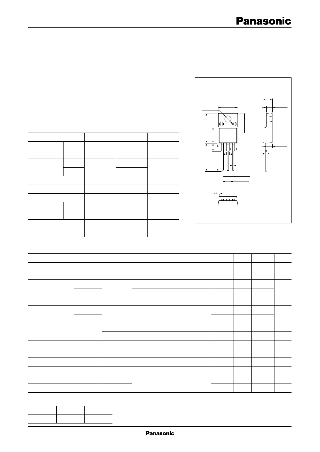
φ3.2±0.1
15.0±0.313.7
–0.2
+0.5
4.1±0.2
8.0±0.2
Solder Dip
7°
min
–60
–80
9.9±0.3
3.0±0.2
1.2±0.15
1.45±0.15
0.75±0.1
2.54±0.2
5.08±0.4
231
TO–220E Full Pack Package
typ
70
10
30
0.5
1.2
0.3
4.6±0.2
max
–200
–200
–300
–300
–1
250
–1.8
–1.2
Unit: mm
2.9±0.2
2.6±0.1
0.7±0.1
1:Base
2:Collector
3:Emitter
Unit
µA
µA
mA
V
V
V
MHz
µs
µs
µs
1
Po wer Transistors 2SB1605, 2SB1605A
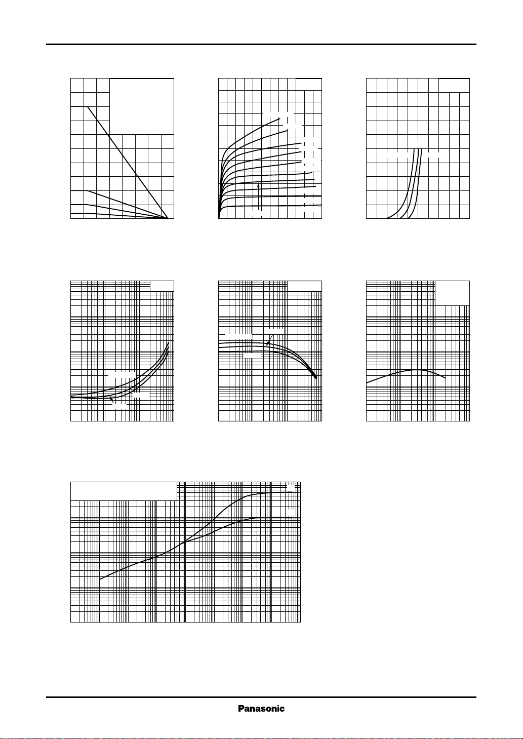
PC—Ta IC—V
50
)
W
(
40
C
30
20
10
Collector power dissipation P
(4)
0
0 16040 12080 14020 10060
Ambient temperature Ta (˚C
)
–100
V
(
–30
CE(sat)
–10
–3
–1
– 0.3
– 0.1
– 0.03
– 0.01
Collector to emitter saturation voltage V
– 0.01
(1) TC=Ta
(2) With a 100 × 100 × 2mm
Al heat sink
(3) With a 50 × 50 × 2mm
Al heat sink
(4) Without heat sink
(P
=2W)
C
(1)
(2)
(3)
V
CE(sat)—IC
=100˚C
T
C
–25˚C
25˚C
– 0.1 –1 –10
– 0.03
– 0.3 –3
Collector current IC (A
)
IC/IB=10
)
CE
–6
–5
)
A
(
–4
C
–3
–2
IB=–100mA
–80mA
Collector current I
–1
0
0 –12–10–8–2 –6–4
–16mA
Collector to emitter voltage VCE (V
hFE—I
C
10000
3000
FE
1000
300
TC=100˚C
100
30
10
Forward current transfer ratio h
3
1
– 0.01
–25˚C
– 0.1 –1 –10
– 0.03
VCE=–4V
25˚C
– 0.3 –3
Collector current IC (A
TC=25˚C
–60mA
–40mA
–30mA
–20mA
–12mA
–8mA
–4mA
)
–10
–8
)
A
(
C
–6
–4
Collector current I
–2
0
0 –2.0–1.6– 0.4 –1.2– 0.8
)
Base to emitter voltage VBE (V
10000
3000
)
MHz
1000
(
T
300
100
30
10
Transition frequency f
3
1
– 0.01
IC—V
BE
V
25˚C
TC=100˚C
– 0.03
–25˚C
fT—I
C
VCE=–5V
f=10MHz
T
– 0.1 –1 –10
– 0.3 –3
Collector current IC (A
CE
=25˚C
C
=–4V
)
)
2
10
(1) Without heat sink
(2) With a 100 × 100 × 2mm Al heat sink
)
˚C/W
(
10
(t)
th
1
–1
10
Thermal resistance R
–2
10
–4
10
–3
2
R
—t
th(t)
(1)
(2)
–1
–2
10
10
Time t (s
1010
110
10
)
3
2
4
10
 Loading...