

Panasonic 2SB1554 Datasheet
Po wer Transistors
2SB1554
Silicon PNP epitaxial planar type
For power amplification
Features
■
●
High forward current transfer ratio hFE which has satisfactory linearity
●
Allowing automatic insertion with radial taping
Absolute Maximum Ratings (T
■
Parameter
Collector to base voltage
Collector to emitter voltage
Emitter to base voltage
Peak collector current
Collector current
Base current
Collector power
dissipation
TC=25°C
Ta=25°C
Junction temperature
Storage temperature
Electrical Characteristics (T
■
Symbol
V
V
V
I
CP
I
C
I
B
P
C
T
j
T
stg
Parameter
Collector cutoff current
Emitter cutoff current
Collector to emitter voltage
Forward current transfer ratio
Collector to emitter saturation voltage
Base to emitter saturation voltage
Transition frequency
Turn-on time
Storage time
Fall time
CBO
CEO
EBO
C
Symbol
I
CBO
I
CEO
I
EBO
V
CEO
*
h
FE1
h
FE2
V
CE(sat)
V
BE(sat)
f
T
t
on
t
stg
t
f
=25˚C)
C
Ratings
–60
–60
–20
–8
–4
–2
15
2
150
–55 to +150
=25˚C)
VCB = –60V, IE = 0
VCE = –50V, IB = 0
VEB = –15V, IC = 0
IC = –10mA, IB = 0
VCE = –4V, IC = – 0.8A
VCE = –4V, IC = –2A
IC = –2A, IB = –100mA
IC = –2A, IB = –100mA
VCE = –10V, IC = – 0.5A, f = 1MHz
IC = –2A,
IB1 = –100mA, IB2 = 100mA,
VCC = –50V
Unit
V
V
V
A
A
A
W
˚C
˚C
Conditions
4.2±0.2
13.0±0.2
18.0±0.5
Solder Dip
C1.0
123
2.5±0.2 2.5±0.2
min
–60
80
30
2.5±0.2
0.65±0.1
1.05±0.10.35±0.1
0.55±0.1
typ
25
0.4
0.6
0.25
1.2±0.1
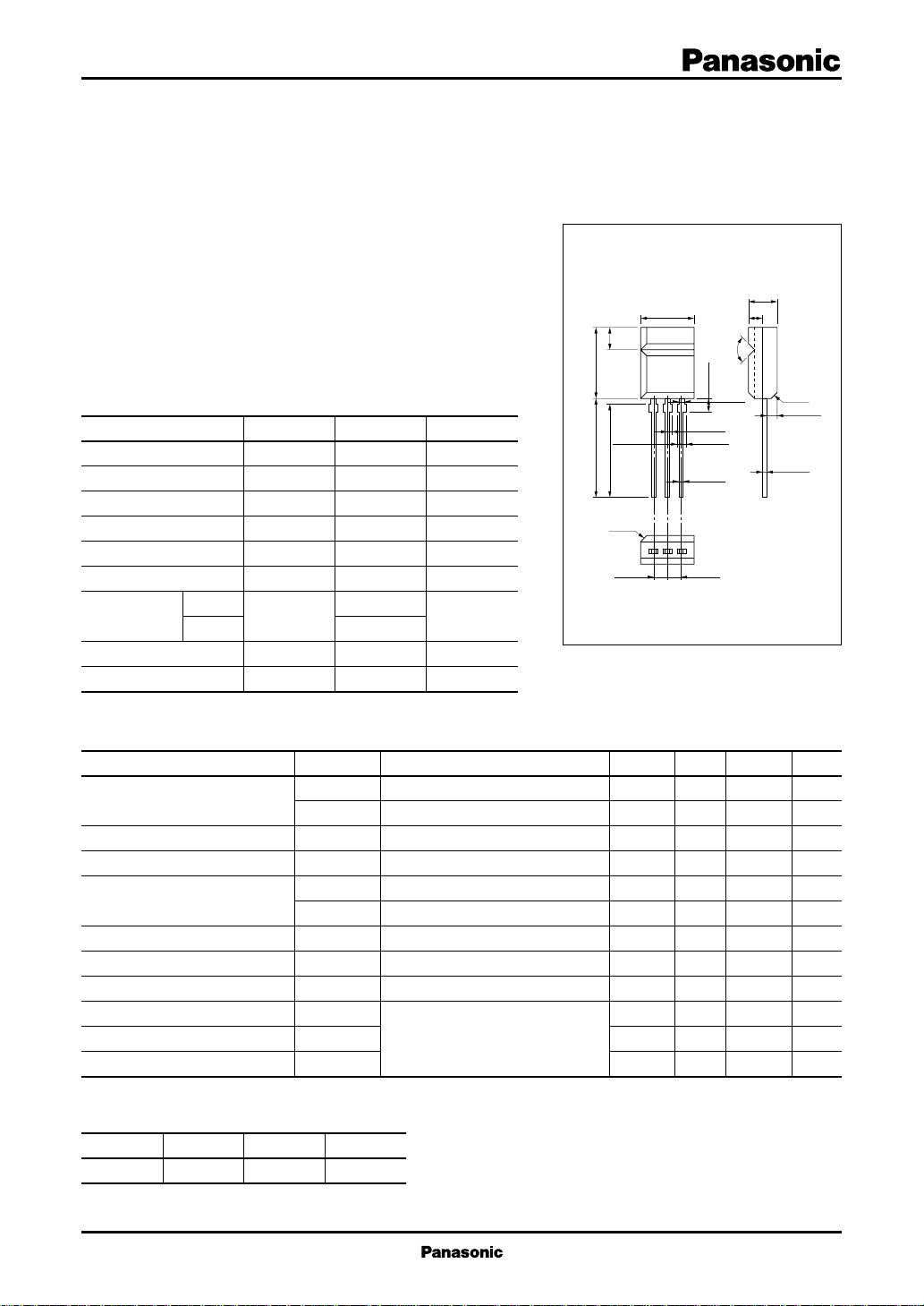
Unit: mm
5.0±0.1
1.010.0±0.2
90°
C1.0
2.25±0.2
0.55±0.1
1:Base
2:Collector
3:Emitter
MT4 Type Package
max
–10
–50
–10
Unit
µA
µA
µA
V
400
–1.0
–1.5
V
V
MHz
µs
µs
µs
*
h
Rank classification
FE1
Rank Q P O
h
FE1
80 to 160 120 to 240 200 to 400
1
Po wer Transistors 2SB1554
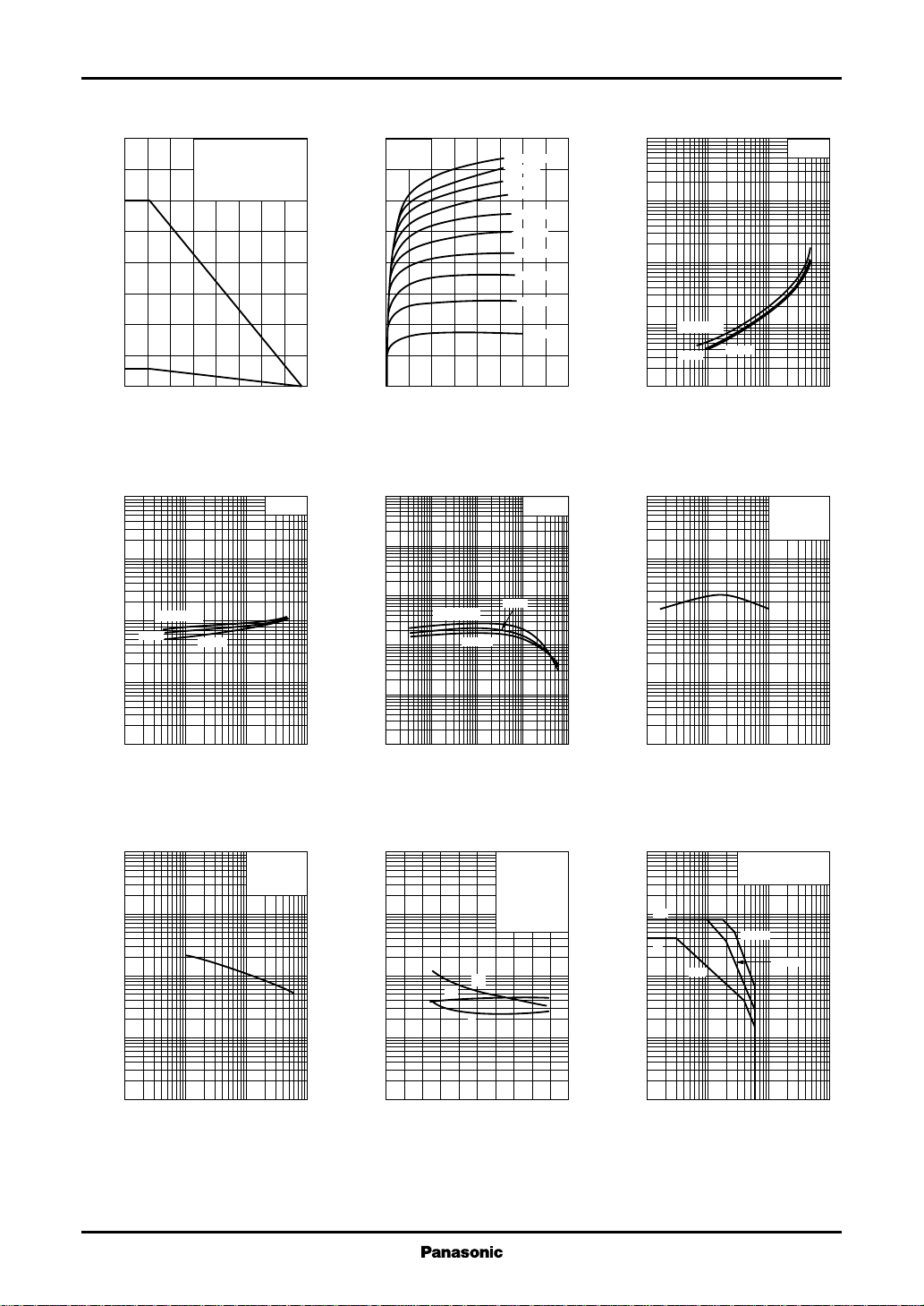
PC—Ta IC—V
20
)
W
(
C
15
10
5
Collector power dissipation P
0
0 16040 12080 14020 10060
Ambient temperature Ta (˚C
–100
)
V
(
–30
BE(sat)
–10
–3
–1
25˚C
– 0.3
– 0.1
– 0.03
Base to emitter saturation voltage V
– 0.01
– 0.01
– 0.03
Collector current IC (A
(1) TC=Ta
(2) Without heat sink
=2.0W)
(P
C
(1)
(2)
V
BE(sat)—IC
TC=–25˚C
100˚C
– 0.1 –1 –10
– 0.3 –3
IC/IB=20
)
CE
)
–4.0
TC=25˚C
–3.5
)
–3.0
A
(
C
–2.5
–2.0
–1.5
–1.0
Collector current I
– 0.5
0
0 –16–4 –12–8 –14–2 –10–6
)
Collector to emitter voltage VCE (V
hFE—I
5
10
FE
4
10
3
10
TC=100˚C
2
10
10
–25˚C
IB=–50mA
–45mA
–40mA
C
25˚C
–35mA
–30mA
–25mA
–20mA
–15mA
–10mA
–5mA
VCE=–4V
Forward current transfer ratio h
1
– 0.001 – 0.01 – 0.1 –1 –10
Collector current IC (A
)
–100
V
(
–30
CE(sat)
–10
–3
–1
– 0.3
– 0.1
– 0.03
– 0.01
Collector to emitter saturation voltage V
)
1000
300
)
MHz
100
(
T
30
10
Transition frequency f
0.3
0.1
V
CE(sat)—IC
TC=100˚C
25˚C
– 0.01
– 0.1 –1 –10
– 0.03
Collector current IC (A
fT—I
3
1
– 0.01
– 0.1 –1 –10
– 0.03
Collector current IC (A
–25˚C
– 0.3 –3
C
VCE=–10V
f=1MHz
T
=25˚C
C
– 0.3 –3
IC/IB=20
)
)
Cob—V
4
10
)
pF
(
ob
3
10
2
10
10
Collector output capacitance C
1
– 0.1 –1 –10 –100– 0.3 –3 –30
Collector to base voltage VCB (V
2
CB
IE=0
f=1MHz
=25˚C
T
C
)
ton, t
100
30
)
µs
(
10
f
,t
stg
3
,t
on
1
0.3
0.1
Switching time t
0.03
0.01
0–5–4–1 –3–2
Collector current IC (A
stg
t
on
, tf—I
Pulsed tw=1ms
Duty cycle=1%
I
(–I
V
T
t
stg
t
f
C/IB
CC
C
C
=20
B1=IB2
=–50V
=25˚C
Area of safe operation (ASO)
–100
)
)
–30
)
I
–10
CP
A
(
C
I
–3
C
–1
– 0.3
– 0.1
Collector current I
– 0.03
– 0.01
–1 –10 –100 –1000–3 –30 –300
Collector to emitter voltage VCE (V
DC
Non repetitive pulse
=25˚C
T
C
t=1ms
10ms
)
 Loading...