

Panasonic 2SB1548, 2SB1548A Datasheet
Po wer Transistors
2SB1548, 2SB1548A
Silicon PNP epitaxial planar type
For power amplification
Complementary to 2SD2374 and 2SD2374A
Features
■
●
High forward current transfer ratio hFE which has satisfactory linearity
●
Low collector to emitter saturation voltage V
●
Full-pack package which can be installed to the heat sink with
one screw
Absolute Maximum Ratings (T
■
Parameter
Collector to
base voltage
Collector to
emitter voltage
2SB1548
2SB1548A
2SB1548
2SB1548A
Emitter to base voltage
Peak collector current
Collector current
Collector power
dissipation
TC=25°C
Ta=25°C
Junction temperature
Storage temperature
Symbol
V
CBO
V
CEO
V
EBO
I
CP
I
C
P
C
T
j
T
stg
CE(sat)
=25˚C)
C
Ratings
–60
–80
–60
–80
–5
–5
–3
25
2
150
–55 to +150
Unit
V
V
V
A
A
W
˚C
˚C
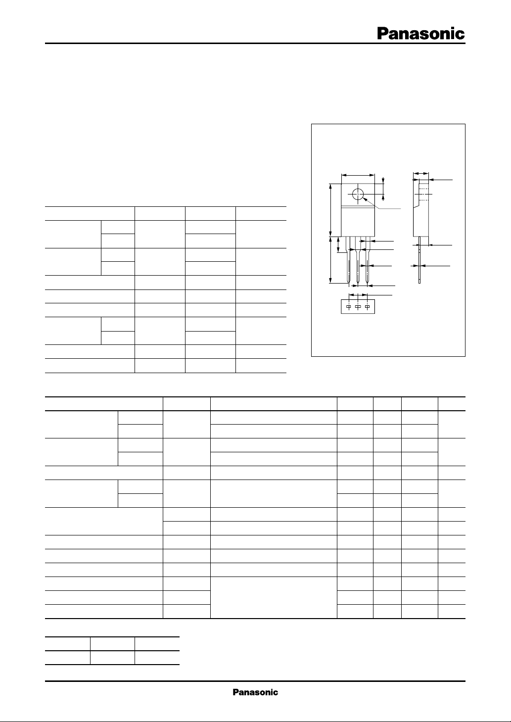
Unit: mm
9.9±0.3
φ3.2±0.1
15.0±0.513.7±0.2
1.4±0.2
1
1.6±0.2
0.8±0.1
2.54±0.3
23
5.08±0.5
TO–220D Full Pack Package
4.2±0.2
4.6±0.2
2.9±0.2
3.0±0.5
2.6±0.1
0.55±0.15
1:Base
2:Collector
3:Emitter
Electrical Characteristics (T
■
Parameter
Collector cutoff
current
Collector cutoff
current
2SB1548
2SB1548A
2SB1548
2SB1548A
Emitter cutoff current
Collector to emitter
voltage
2SB1548
2SB1548A
Forward current transfer ratio
Base to emitter voltage
Collector to emitter saturation voltage
Transition frequency
Turn-on time
Storage time
Fall time
*
h
Rank classification
FE1
C
Symbol
I
CES
I
CEO
I
EBO
V
CEO
*
h
FE1
h
FE2
V
BE
V
CE(sat)
f
T
t
on
t
stg
t
f
=25˚C)
VCE = –60V, VBE = 0
VCE = –80V, VBE = 0
VCE = –30V, IB = 0
VCE = –60V, IB = 0
VEB = –5V, IC = 0
IC = –30mA, IB = 0
VCE = –4V, IC = –1A
VCE = –4V, IC = –3A
VCE = –4V, IC = –3A
IC = –3A, IB = – 0.375A
VCE = –10V, IC = – 0.5A, f = 10MHz
IC = –1A, IB1 = – 0.1A, IB2 = 0.1A
Rank Q P
h
FE1
70 to 150 120 to 250
Note: Ordering can be made by the common rank (PQ rank h
Conditions
= 70 to 250) in the rank classification.
FE1
min
–60
–80
70
10
typ
30
0.5
1.2
0.3
max
–200
–200
–300
–300
–1
250
–1.8
–1.2
Unit
µA
µA
mA
V
V
V
MHz
µs
µs
µs
1
Po wer Transistors 2SB1548, 2SB1548A
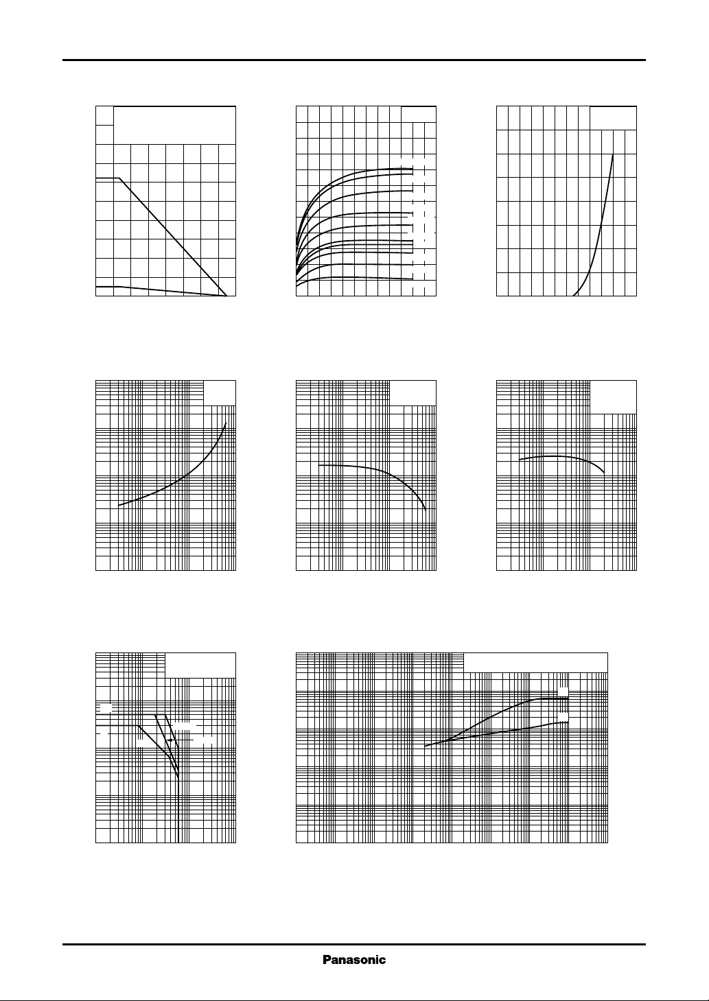
PC—Ta IC—V
40
)
W
(
C
Collector power dissipation P
)
–10
V
(
CE(sat)
– 0.3
– 0.1
(1) TC=Ta
36
(2) Without heat sink (P
32
28
(1)
24
20
16
12
8
4
(2)
0
0 16040 12080 14020 10060
Ambient temperature Ta (˚C
V
CE(sat)—IC
–3
–1
=2W)
C
IC/IB=10
=25˚C
T
C
CE
–6
–5
)
A
(
–4
C
–3
–2
Collector current I
–1
0
0 –12–10–8–2 –6–4
)
Collector to emitter voltage VCE (V
hFE—I
10000
3000
FE
1000
300
100
C
TC=25˚C
IB=–100mA
–80mA
–60mA
–40mA
–30mA
–20mA
–16mA
–12mA
–8mA
–4mA
VCE=–4V
=25˚C
T
C
)
–8
–7
)
–6
A
(
C
–5
–4
–3
–2
Collector current I
–1
0
0 –1.2–1.0– 0.8– 0.2 – 0.6– 0.4
Base to emitter voltage VBE (V
1000
300
)
MHz
100
(
T
30
10
IC—V
fT—I
BE
C
VCE=–4V
=25˚C
T
C
VCE=–10V
f=10MHz
T
=25˚C
C
)
– 0.03
– 0.01
– 0.003
– 0.001
Collector to emitter saturation voltage V
– 0.01
– 0.1 –1 –10
– 0.03
– 0.3 –3
Collector current IC (A
)
30
10
Forward current transfer ratio h
3
1
– 0.01
– 0.1 –1 –10
– 0.03
– 0.3 –3
Collector current IC (A
Area of safe operation (ASO) R
–100
–30
)
–10
A
(
I
CP
C
–3
I
C
–1
– 0.3
– 0.1
Collector current I
– 0.03
– 0.01
–1 –10 –100 –1000–3 –30 –300
Non repetitive pulse
T
DC
=25˚C
C
t=1ms
10ms
Collector to emitter voltage VCE (V
)
3
10
)
2
10
˚C/W
(
(t)
th
10
1
–1
10
Thermal resistance R
–2
10
–4
10
–3
–2
10
)
–1
10
3
1
Transition frequency f
0.3
0.1
– 0.01
—t
th(t)
(1) Without heat sink
(2) With a 100 × 80 × t2mm Al heat sink
1010
110
Time t (s
)
– 0.1 –1 –10
– 0.03
– 0.3 –3
Collector current IC (A
(1)
(2)
3
2
10
)
4
10
2
 Loading...