

Panasonic 2SB1488 Datasheet
Transistor
2SB1488
Silicon PNP triple diffusion planer type
For power switching
Features
■
●
High foward current transfer ratio hFE.
●
High-speed switching.
●
High collector to base voltage V
●
Allowing supply with the radial taping.
Absolute Maximum Ratings (Ta=25˚C)
■
Parameter
Collector to base voltage
Collector to emitter voltage
Emitter to base voltage
Peak collector current
Collector current
Collector power dissipation
Junction temperature
Storage temperature
*
Printed circuit board: Copper foil area of 1cm2 or more, and the board
thickness of 1.7mm for the collector portion
Symbol
V
V
V
I
CP
I
C
P
C
T
j
T
stg
CBO
CEO
EBO
CBO
.
Ratings
–400
–400
–7
–1
– 0.5
1
150
–55 ~ +150
Unit
V
V
V
A
A
W
˚C
˚C
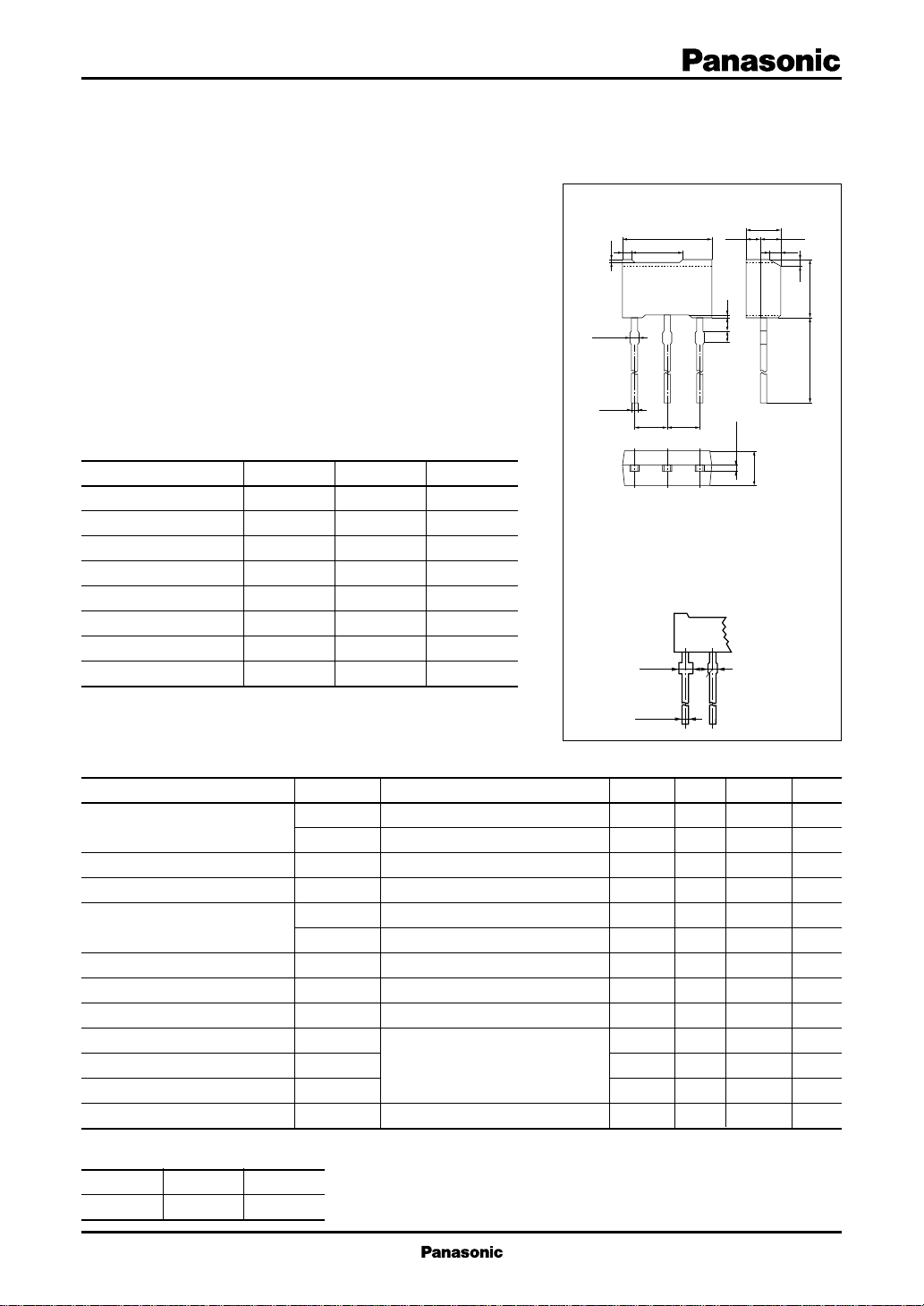
6.9±0.1
4.00.7 0.8
0.15
0.65 max.
+0.1
0.45
–0.05
2.5±0.5 2.5±0.5
Note: In addition to the
lead type shown in
the upper figure, the
type as shown in
the lower figure is
also available.
1.2±0.1
+
0.1
0.45
–
0.05
1.05
±0.05 (1.45)
0.21.01.0
–0.05
+0.1
321
0.45
1:Emitter
2:Collector
3:Base
MT2 Type Package
0.65
max.
Unit: mm
2.5±0.1
0.5
4.5±0.114.5±0.5
2.5±0.1
(HW type)
Electrical Characteristics (Ta=25˚C)
■
Parameter
Collector cutoff current
Emitter cutoff current
Collector to emitter voltage
Forward current transfer ratio
Collector to emitter saturation voltage
Base to emitter saturation voltage
Transition frequency
Turn-on time
Storage time
Collector current fall time
Collector output capacitance
*1
h
Rank classification
FE1
Symbol
I
CBO
I
CEO
I
EBO
V
CEO
h
FE1
h
FE2
V
CE(sat)
V
BE(sat)
f
T
t
on
t
stg
t
f
C
ob
Rank P Q
h
FE1
80 ~ 160 130 ~ 280
Conditions
VCB = –400V, IE = 0
VCE = –100V, IB = 0
VBE = –5V, IC = 0
IC = –1mA, IB = 0
*1
VCE = –5V, IC = –50mA
VCE = –5V, IC = –300mA
IC = –100mA, IB = –10mA
IC = –100mA, IB = –10mA
*2
*2
*2
VCB = –10V, IE = 0.1A, f = 1MHz
IC = –100mA, RL = 1.5kΩ
IB1 = –10mA, IB2 = 10mA
VCC = –150V
VCB = –10V, IE = 0, f = 1MHz
min
–400
80
typ
max
–1
–1
–1
280
Unit
µA
µA
µA
V
10
– 0.25
– 0.8
*2
0.4
5.5
0.5
– 0.5
–1.2
25
1.0
6.5
1.0
20
40
*2
Pulse measurement
V
V
MHz
µs
µs
µs
pF
1
Transistor
2SB1488
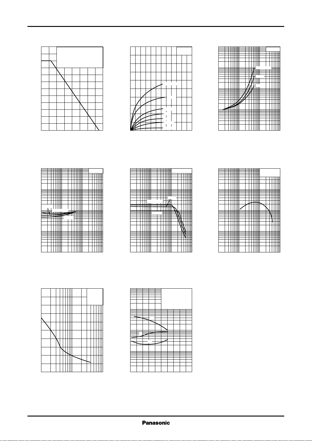
PC — Ta IC — V
1.2
)
W
(
1.0
C
0.8
0.6
0.4
0.2
Collector power dissipation P
0
–100
)
V
(
–30
BE(sat)
–10
–3
–1
– 0.3
– 0.1
– 0.03
Base to emitter saturation voltage V
– 0.01
– 0.01
Printed circut board: Copper
foil area of 1cm
the board thickness of 1.7mm
for the collector portion.
0 16040 12080 14020 10060
2
or more, and
Ambient temperature Ta (˚C
V
— I
BE(sat)
25˚C
Ta=–25˚C
100˚C
– 0.1 –1 –10
– 0.03
C
– 0.3 –3
Collector current IC (A
IC/IB=5
)
V
CE
)
–1.0
– 0.9
– 0.8
)
mA
(
– 0.7
C
– 0.6
– 0.5
– 0.4
– 0.3
Collector current I
– 0.2
– 0.1
0
0 –12–10–8–2 –6–4
)
Collector to emitter voltage VCE (V
hFE — I
10000
3000
FE
1000
300
100
30
10
Forward current transfer ratio h
3
1
– 0.001
Ta=100˚C
–25˚C
– 0.01
– 0.003
– 0.03
Collector current IC (A
Ta=25˚C
=100mA
I
B
50mA
10mA
5mA
1mA
0.5mA
0.1mA
C
VCE=–5V
25˚C
– 0.1 –1
– 0.3
)
–100
V
(
–30
CE(sat)
–10
–3
–1
– 0.3
– 0.1
– 0.03
– 0.01
Collector to emitter saturation voltage V
– 0.01
– 0.03
)
Collector current IC (A
1000
300
)
MHz
100
(
T
30
10
3
1
Transition frequency f
0.3
0.1
– 0.001
– 0.003
Collector current IC (A
— I
CE(sat)
– 0.1 –1 –10
C
IC/IB=5
Ta=100˚C
25˚C
–25˚C
– 0.3 –3
)
fT — I
C
VCE=–10V
Ta=25˚C
– 0.01
– 0.03
– 0.1 –1
– 0.3
)
Cob — V
100
)
90
pF
(
80
ob
70
60
50
40
30
20
10
Collector output capacitance C
0
–1 –3 –10 –30 –100
CB
Collector to base voltage VCB (V
2
IE=0
f=1MHz
Ta=25˚C
)
ton, t
100
30
)
µs
(
10
f
,t
stg
3
,t
on
1
t
f
0.3
0.1
Switching time t
0.03
0.01
0 – 1.0– 0.8– 0.2 – 0.6– 0.4
Collector current IC (A
t
t
on
stg
stg
, tf — I
Pulsed tw=1ms
Duty cycle=1%
I
C/IB
V
CC
Ta=25˚C
C
=5(–IB1=IB2)
=–100V
)
 Loading...