

Panasonic 2SB1462 Datasheet
Transistor
2SB1462
Silicon PNP epitaxial planer type
For general amplification
Complementary to 2SD2216
Features
■
●
High foward current transfer ratio hFE.
●
SS-Mini type package, allowing downsizing of the equipment
and automatic insertion through the tape packing and the magazine packing.
Absolute Maximum Ratings (Ta=25˚C)
■
Parameter
Collector to base voltage
Collector to emitter voltage
Emitter to base voltage
Peak collector current
Collector current
Collector power dissipation
Junction temperature
Storage temperature
Electrical Characteristics (Ta=25˚C)
■
Parameter
Collector cutoff current
Collector to base voltage
Collector to emitter voltage
Emitter to base voltage
Forward current transfer ratio
Collector to emitter saturation voltage
Transition frequency
Collector output capacitance
Symbol
V
CBO
V
CEO
V
EBO
I
CP
I
C
P
C
T
j
T
stg
Symbol
I
CBO
I
CEO
V
CBO
V
CEO
V
EBO
*
h
FE
V
CE(sat)
f
T
C
ob
Ratings
–60
–50
–7
–200
–100
125
125
–55 ~ +125
VCB = –20V, IE = 0
VCE = –10V, IB = 0
IC = –10µA, IE = 0
IC = –100µA, IB = 0
IE = –10µA, IC = 0
VCE = –10V, IC = –2mA
IC = –100mA, IB = –10mA
VCB = –10V, IE = 1mA, f = 200MHz
VCB = –10V, IE = 0, f = 1MHz
Unit
V
V
V
mA
mA
mW
˚C
˚C
Conditions
1.6±0.15
0.8±0.1 0.40.4
1
0.5
1.6±0.1
1.0±0.1
0.5
2
0.3
0.75±0.15
0.45±0.1
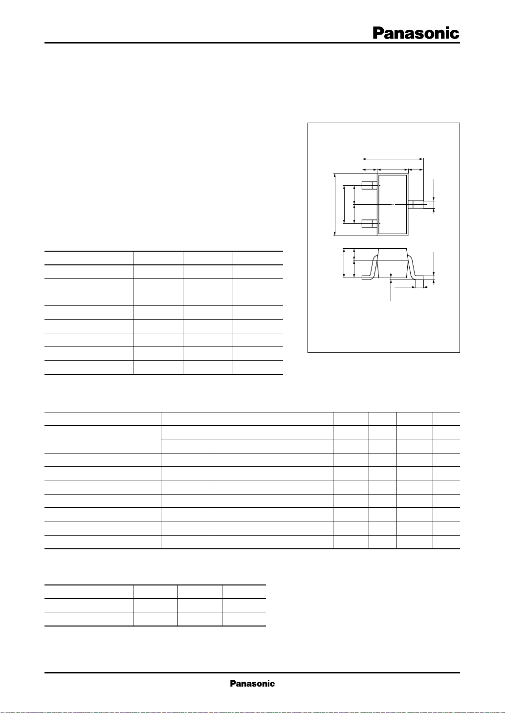
1:Base
2:Emitter EIAJ:SC–75
3:Collector SS-Mini Type Package
0.2±0.1
0 to 0.1
Marking symbol : A
min
–60
–50
–7
160
typ
– 0.11
80
2.7
max
– 0.1
–100
460
– 0.3
Unit: mm
3
+0.1
+0.1
–0.05
0.2
–0.05
0.15
Unit
µA
µA
V
V
V
V
MHz
pF
*
hFE Rank classification
Rank Q R S
h
FE
160 ~ 260 210 ~ 340 290 ~ 460
Marking Symbol AQ AR AS
1
Transistor 2SB1462
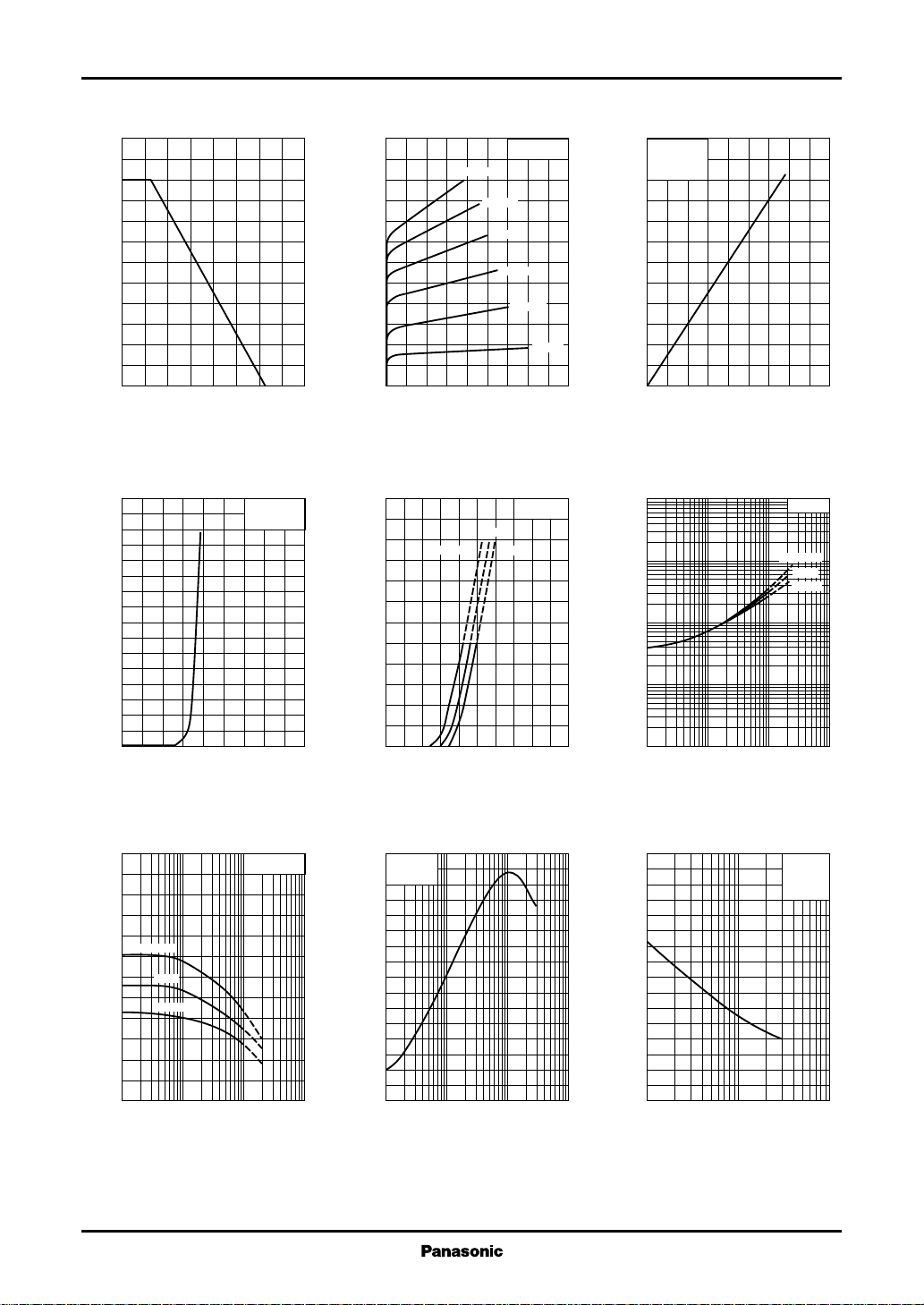
PC — Ta IC — V
150
)
mW
125
(
C
100
75
50
25
Collector power dissipation P
0
0 16040 12080 14020 10060
Ambient temperature Ta (˚C
IB — V
BE
–400
–350
–300
)
µA
(
–250
B
–200
VCE=–5V
Ta=25˚C
CE
–60
–50
)
mA
(
–40
C
–30
–20
Collector current I
–10
0
0 –18–6 –12
)
Collector to emitter voltage VCE (V
IB=–300µA
IC — V
–240
–200
)
mA
(
–160
C
–120
Ta=75˚C
Ta=25˚C
–250µA
–200µA
–150µA
–100µA
–50µA
BE
VCE=–5V
25˚C
–25˚C
–60
–50
)
mA
(
–40
C
–30
–20
Collector current I
–10
)
)
–10
V
(
CE(sat)
– 0.3
– 0.1
0
0 –450–150 –300
–3
–1
IC — I
VCE=–5V
Ta=25˚C
Base current IB (µA
V
— I
CE(sat)
B
)
C
IC/IB=10
Ta=75˚C
25˚C
–25˚C
–150
Base current I
–100
–50
0
0 –1.8– 0.6 –1.2
Base to emitter voltage VBE (V
hFE — I
C
600
FE
500
400
Ta=75˚C
300
200
100
Forward current transfer ratio h
25˚C
–25˚C
0
–1 –10 –100 –1000–3 –30 –300
VCE=–10V
Collector current IC (mA
–80
Collector current I
–40
0
0 –2.0–1.6– 0.4 –1.2– 0.8
)
)
Base to emitter voltage VBE (V
fT — I
E
160
VCB=–10V
Ta=25˚C
140
)
MHz
120
(
T
100
80
60
40
Transition frequency f
20
0
0.1 1 10 1000.3 3 30
Emitter current IE (mA
)
)
– 0.03
– 0.01
– 0.003
– 0.001
Collector to emitter saturation voltage V
–1 –10 –100 –1000–3 –30 –300
Collector current IC (mA
Cob — V
8
)
pF
7
(
ob
6
5
4
3
2
1
Collector output capacitance C
0
–1 –3 –10 –30 –100
CB
)
IE=0
f=1MHz
Ta=25˚C
Collector to base voltage VCB (V
)
2
 Loading...