

Panasonic 2SB1319 Datasheet
Transistor
2SB1319
Silicon PNP epitaxial planer type
For low-frequency power amplification
Features
■
●
Low collector to emitter saturation voltage V
●
Large collector current IC.
●
M type package allowing easy automatic and manual insertion as
well as stand-alone fixing to the printed circuit board.
Absolute Maximum Ratings (Ta=25˚C)
■
Parameter
Collector to base voltage
Collector to emitter voltage
Emitter to base voltage
Peak collector current
Collector current
Collector power dissipation
Junction temperature
Storage temperature
*
Printed circuit board: Copper foil area of 1cm2 or more, and the board
thickness of 1.7mm for the collector portion
Symbol
V
CBO
V
CEO
V
EBO
I
CP
I
C
*
P
C
T
j
T
stg
Ratings
–30
–20
–7
–8
–5
150
–55 ~ +150
1
CE(sat)
.
Unit
V
V
V
A
A
W
˚C
˚C
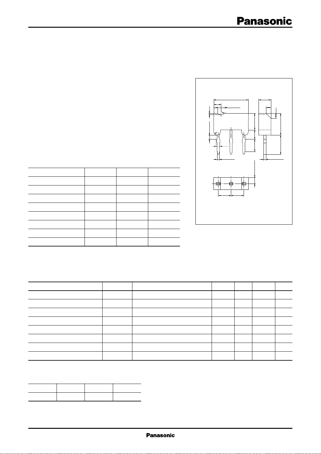
6.9±0.1
1.5
1.5 R0.9
0.4
R0.9
R0.7
1.0±0.1
0.85
0.55±0.1 0.45±0.05
2.5 2.5
1:Base
2:Collector EIAJ:SC–71
3:Emitter M Type Mold Package
2.5±0.1
3.5±0.1
2.0±0.2
2.4±0.21.25±0.05
123
Unit: mm
1.0
1.0
4.1±0.2 4.5±0.1
Electrical Characteristics (Ta=25˚C)
■
Parameter
Collector cutoff current
Emitter cutoff current
Collector to emitter voltage
Emitter to base voltage
Forward current transfer ratio
Collector to emitter saturation voltage
Transition frequency
Collector output capacitance
*1
hFE Rank classification
Symbol
I
CBO
I
EBO
V
CEO
V
EBO
h
FE
V
CE(sat)
f
T
C
ob
Rank P Q R
h
FE
90 ~ 135 120 ~ 205 180 ~ 625
Conditions
VCB = –10V, IE = 0
VEB = –5V, IC = 0
IC = –1mA, IB = 0
IE = –10µA, IC = 0
*1
VCE = –2V, IC = –2A
IC = –3A, IB = –0.1A
*2
*2
VCB = –6V, IE = 50mA, f = 200MHz
VCB = –20V, IE = 0, f = 1MHz
min
–20
–7
90
typ
max
–100
–1
625
–1
120
85
*2
Pulse measurement
Unit
nA
µA
V
V
V
MHz
pF
1
Transistor
2SB1319
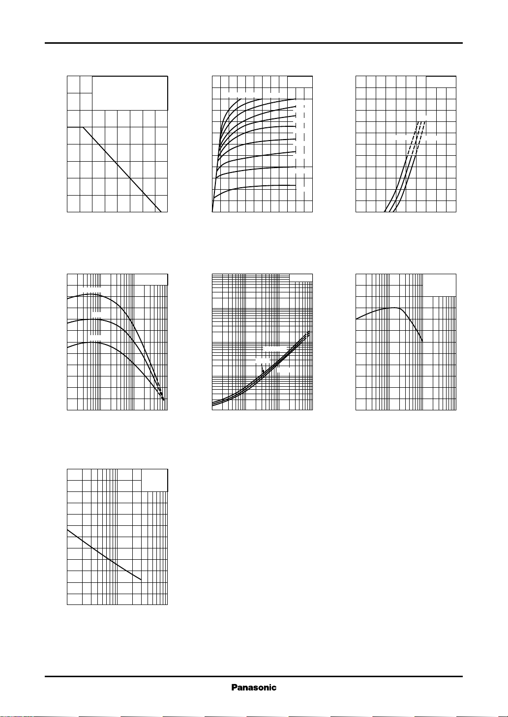
PC — Ta IC — V
1.6
)
1.4
W
(
C
1.2
1.0
0.8
0.6
0.4
0.2
Collector power dissipation P
0
600
FE
500
400
300
200
100
Forward current transfer ratio h
0
– 0.01
Printed circut board: Copper
foil area of 1cm
the board thickness of 1.7mm
for the collector portion.
0 16040 12080 14020 10060
2
or more, and
Ambient temperature Ta (˚C
hFE — I
C
VCE=–2V
Ta=75˚C
25˚C
–25˚C
– 0.1 –1 –10
– 0.03
– 0.3 –3
Collector current IC (A
CE
–6
IB=–50mA
–5
)
A
(
–4
C
–3
–2
–45mA
Ta=25˚C
–40mA
–35mA
–30mA
–25mA
–20mA
–15mA
–10mA
Collector current I
–1
0
0–6–5–4–1 –3–2
)
)
Collector to emitter voltage VCE (V
V
— I
CE(sat)
)
–100
V
(
–30
CE(sat)
–10
–3
–1
– 0.3
– 0.1
– 0.03
– 0.01
Collector to emitter saturation voltage V
– 0.01
– 0.03
Ta=75˚C
25˚C
– 0.1 –1 –10
– 0.3 –3
Collector current IC (A
–5mA
C
IC/IB=30
–25˚C
)
–12
–10
)
A
(
–8
C
–6
–4
Collector current I
–2
0
0 –2.0–1.6– 0.4 –1.2– 0.8
)
240
)
200
MHz
(
T
160
120
80
40
Transition frequency f
0
1 10 100 10003 30 300
IC — V
BE
VCE=–2V
25˚C
Ta=75˚C
–25˚C
Base to emitter voltage VBE (V
fT — I
E
VCB=–6V
Ta=25˚C
Emitter current IE (mA
)
)
Cob — V
300
)
pF
(
250
ob
200
150
100
50
Collector output capacitance C
0
–1 –3 –10 –30 –100
Collector to base voltage VCB (V
2
CB
IE=0
f=1MHz
Ta=25˚C
)
 Loading...