

Panasonic 2SA1790 Datasheet
Transistor
2SA1790
Silicon PNP epitaxial planer type
For high-frequency amplification
Complementary to 2SC4626
Features
■
●
High transition frequency fT.
●
SS-Mini type package, allowing downsizing of the equipment
and automatic insertion through the tape packing and the magazine packing.
Absolute Maximum Ratings (Ta=25˚C)
■
Parameter
Collector to base voltage
Collector to emitter voltage
Emitter to base voltage
Collector current
Collector power dissipation
Junction temperature
Storage temperature
Electrical Characteristics (Ta=25˚C)
■
Parameter
Collector cutoff current
Emitter cutoff current
Forward current transfer ratio
Transition frequency
Collector to emitter saturation voltage
Base to emitter voltage
Noise figure
Reverse transfer impedance
Common emitter reverse transfer
capacitance
Symbol
V
CBO
V
CEO
V
EBO
I
C
P
C
T
j
T
stg
Symbol
I
CBO
I
CEO
I
EBO
*
h
FE
f
T
V
CE(sat)
V
BE
NF
Z
rb
C
re
Ratings
–30
–20
–5
–30
125
125
–55 ~ +125
VCB = –10V, IE = 0
VCE = –20V, IB = 0
VEB = –5V, IC = 0
VCE = –10V, IC = 1mA
VCB = –10V, IE = 1mA, f = 200MHz
IC = –10mA, IB = –1mA
VCE = –10V, IC = –1mA
VCB = –10V, IE = 1mA, f = 5MHz
VCB = –10V, IE = 1mA, f = 2MHz
VCE = –10V, IC = –1mA
f = 10.7MHz
Unit
V
V
V
mA
mW
˚C
˚C
Conditions
1.6±0.15
0.8±0.1 0.40.4
1
0.5
1.6±0.1
1.0±0.1
0.5
2
0.3
0.75±0.15
0.45±0.1
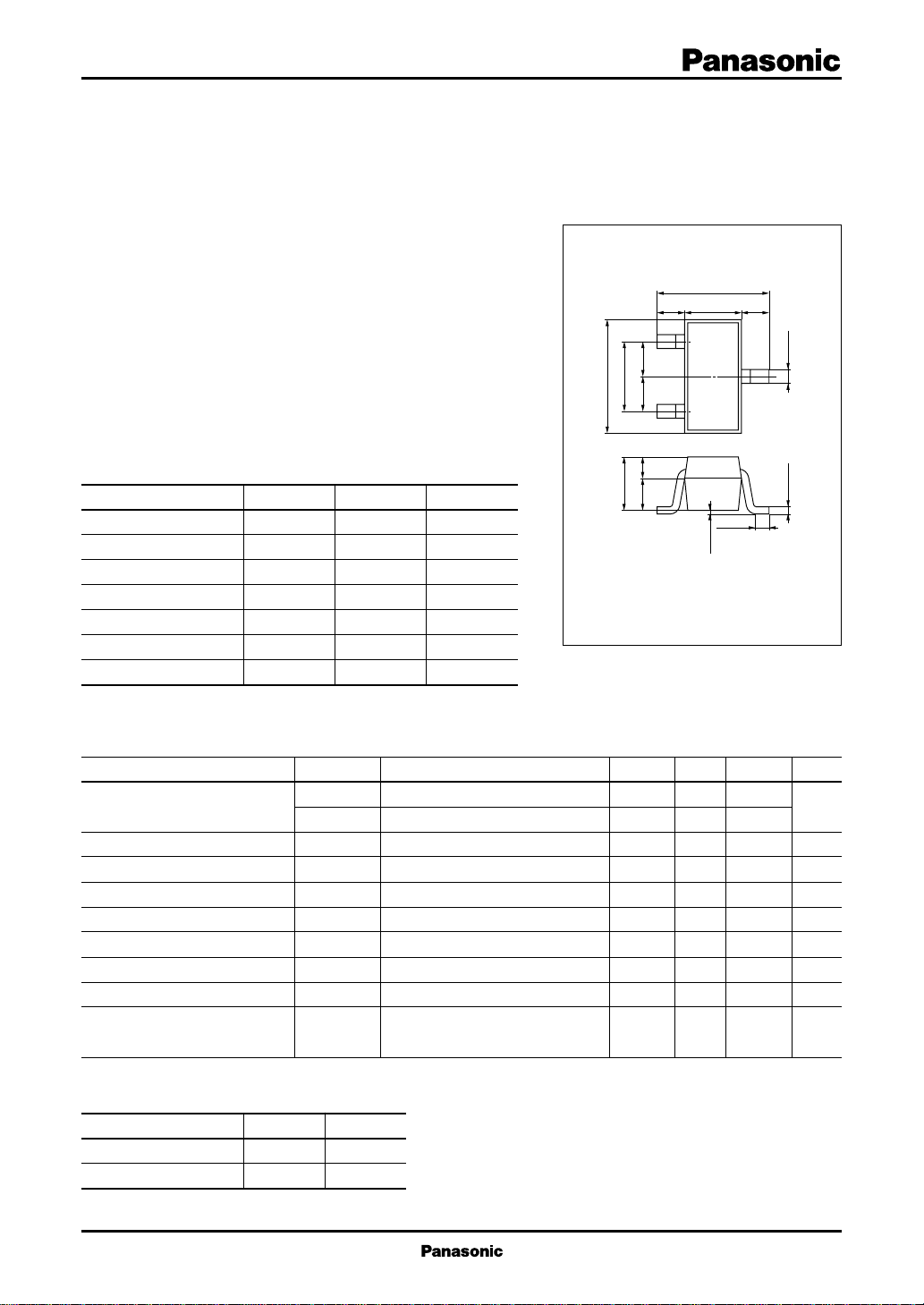
1:Base
2:Emitter EIAJ:SC–75
3:Collector SS–Mini Type Package
0.2±0.1
0 to 0.1
Marking symbol : E
min
70
150
typ
300
– 0.1
– 0.7
2.8
22
1.2
max
– 0.1
–100
–10
220
4.0
60
2.0
3
Unit: mm
–0.05
+0.1
0.2
–0.05
+0.1
0.15
Unit
µA
µA
MHz
dB
pF
V
V
Ω
*
hFE Rank classification
Rank B C
h
FE
70 ~ 140 110 ~ 220
Marking Symbol EB EC
1
Transistor
2SA1790
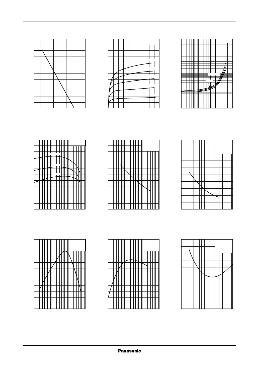
PC—Ta IC—V
150
)
mW
125
(
C
100
75
50
25
Collector power dissipation P
0
0 16040 12080 14020 10060
Ambient temperature Ta (˚C
hFE—I
C
120
FE
100
80
60
40
Ta=75˚C
25˚C
–25˚C
VCE=–10V
CE
)
–30
–25
)
mA
(
–20
C
–15
–10
Collector current I
–5
0
0 –10–8–2 –6–4
)
Collector to emitter voltage VCE (V
Cob—V
6
)
pF
(
5
ob
4
3
2
CB
Ta=25˚C
IB=–250µA
–200µA
–150µA
–100µA
–50µA
f=1MHz
I
=0
E
Ta=25˚C
–100
V
(
–30
CE(sat)
–10
–3
–1
– 0.3
– 0.1
– 0.03
– 0.01
Collector to emitter saturation voltage V
)
)
pF
(
re
V
CE(sat)—IC
IC/IB=10
Ta=75˚C
25˚C
–25˚C
– 0.1 –1 –10 –100– 0.3 –3 –30
Collector current IC (mA
Cre—V
5
4
3
2
CE
IC=–1mA
f=10.7MHz
Ta=25˚C
)
20
Forward current transfer ratio h
0
– 0.1 –1 –10 –100– 0.3 –3 –30
Collector current IC (mA
fT—I
E
600
)
500
MHz
(
T
400
300
200
100
Transition frequency f
0
0.1 1 10 1000.3 3 30
VCB=–10V
Ta=25˚C
Emitter current IE (mA
1
1
Collector output capacitance C
0
– 0.1 –1 –10 –100– 0.3 –3 –30
)
Collector to base voltage VCB (V
PG — I
C
24
20
VCE=–10V
f=100MHz
Ta=25˚C
)
dB
(
16
12
8
Power gain PG
4
0
– 0.1 –1 –10 –100– 0.3 –3 –30
)
Collector current IC (mA
)
Common emitter reverse transfer capacitance C
0
–1 –3 –10 –30 –100
)
Collector to emitter voltage VCE (V
NF — I
E
5
4
)
dB
(
3
2
Noise figure NF
1
0
0.1 0.3 1 3 10
VCB=–10V
f=100MHz
Ta=25˚C
Emitter current IE (mA
)
)
2
 Loading...