

Panasonic 2SA1535A, 2SA1535 Datasheet
Po wer Transistors
10.0±0.2
5.5±0.2
7.5±0.2
16.7±0.3
0.7±0.1
14.0±0.5
Solder Dip
4.0
0.5
+0.2
–0.1
1.4±0.1
1.3±0.2
0.8±0.1
2.54±0.25
5.08±0.5
213
2.7±0.2
4.2±0.2
4.2±0.2
φ3.1±0.1
2SA1535, 2SA1535A
Silicon PNP epitaxial planar type
For low-frequency driver and high power amplification
Complementary to 2SC3944 and 2SC3944A
Features
■
●
Satisfactory foward current transfer ratio hFE vs. collector current I
characteristics
●
●
■
C
High transition frequency f
T
Makes up a complementary pair with 2SC3944 and 2SC3944A,
which is optimum for the driver-stage of a 60 to 100W output
amplifier.
Absolute Maximum Ratings (T
Parameter
Collector to
base voltage
Collector to
emitter voltage
2SA1535
2SA1535A
2SA1535
2SA1535A
Emitter to base voltage
Peak collector current
Collector current
Collector power
dissipation
TC=25°C
Ta=25°C
Junction temperature
Storage temperature
Symbol
V
CBO
V
CEO
V
EBO
I
CP
I
C
P
C
T
j
T
stg
=25˚C)
C
Ratings
–150
–180
–150
–180
–5
–1.5
–1
15
2.0
150
–55 to +150
Unit
V
V
V
A
A
W
˚C
˚C
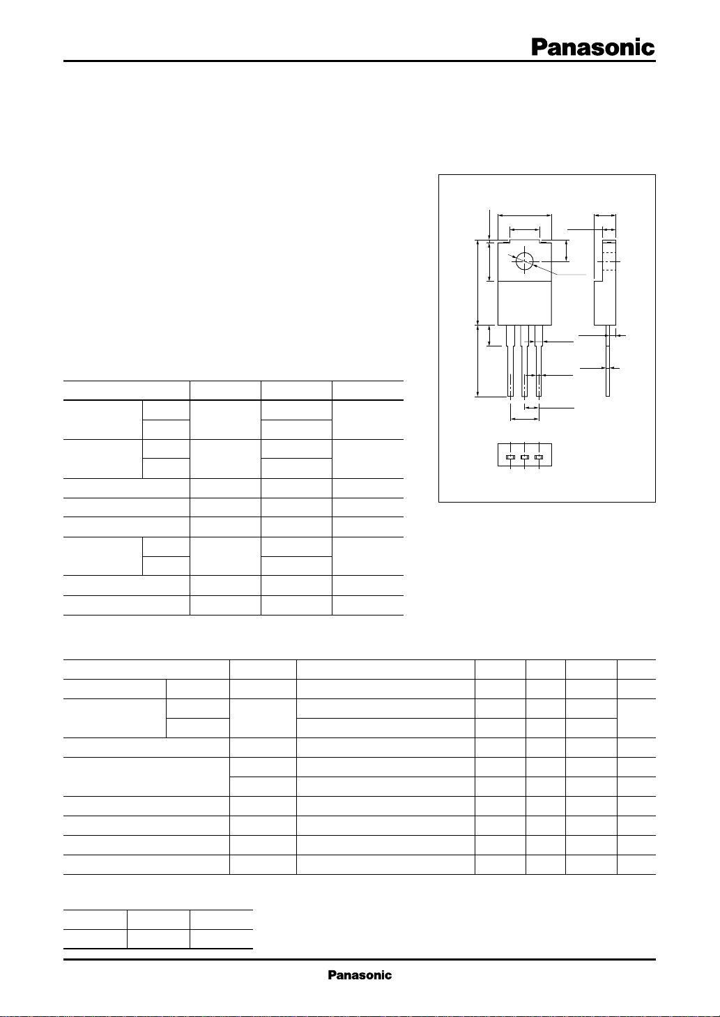
Unit: mm
1:Base
2:Collector
3:Emitter
TO–220 Full Pack Package(a)
Electrical Characteristics (T
■
Parameter
Collector cutoff current
Collector to emitter
voltage
Emitter to base voltage
Forward current transfer ratio
Collector to emitter saturation voltage
Base to emitter saturation voltage
Transition frequency
Collector output capacitance
*
h
Rank classification
FE1
Rank Q R
h
FE1
90 to 155 130 to 220
2SA1535
2SA1535
2SA1535A
C
Symbol
I
CBO
V
CEO
V
EBO
h
*
FE1
h
FE2
V
CE(sat)
V
BE(sat)
f
T
C
ob
=25˚C)
Conditions
VCB = –150V, IE = 0
IC = –1mA, IB = 0
IC = –100µA, IB = 0
IE = –10µA, IC = 0
VCE = –10V, IC = –150mA
VCE = –5V, IC = –500mA
IC = –500mA, IB = –50mA
IC = –500mA, IB = –50mA
VCE = –10V, IC = –50mA, f = 10MHz
VCB = –10V, IE = 0, f = 1MHz
min
–150
–180
–5
90
50
typ
160
100
– 0.5
–1.0
200
30
max
–10
220
–2.0
–2.0
50
Unit
µA
V
V
V
V
MHz
pF
1
Po wer Transistors 2SA1535, 2SA1535A
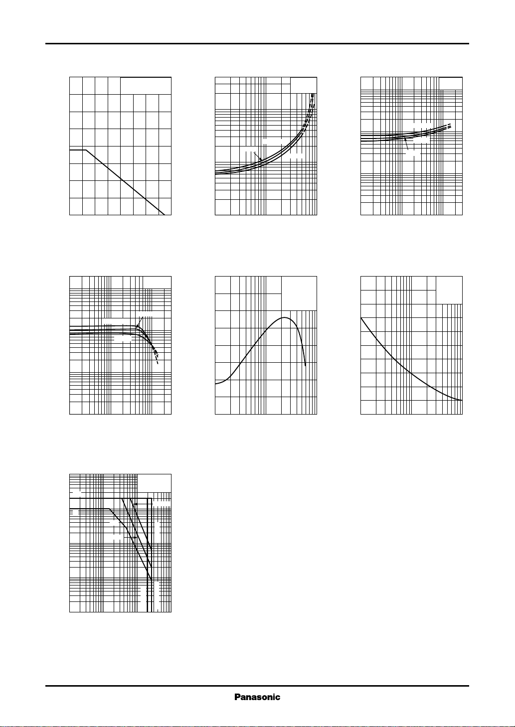
PC—Ta V
32
)
28
W
(
C
24
20
16
12
8
4
Collector power dissipation P
0
0 16040 12080 14020 10060
Ambient temperature Ta (˚C
1000
FE
300
100
30
10
3
Forward current transfer ratio h
1
– 0.01 –3–1– 0.1– 0.03 – 0.3
Collector current IC (A
Without heat sink
hFE—I
TC=–25˚C
100˚C
C
VCE=–10V
25˚C
)
CE(sat)—IC
V
(
–3
CE(sat)
–1
– 0.3
– 0.1
– 0.03
– 0.01
Collector to emitter saturation voltage V
– 0.01 – 0.03 – 0.1 – 0.3 –1
)
Collector current IC (A
25˚C
TC=100˚C
fT—I
400
)
MHz
300
(
T
200
100
E
IC/IB=10
–25˚C
)
VCB=–10V
f=10MHz
=25˚C
T
C
Transition frequency f
)
V
(
–10
BE(sat)
–3
–1
– 0.3
– 0.1
– 0.03
Base to emitter saturation voltage V
– 0.01
– 0.01 –3–1– 0.1– 0.03 – 0.3
100
)
pF
(
80
ob
60
40
20
V
BE(sat)—IC
TC=–25˚C
100˚C
25˚C
Collector current IC (A
Cob—V
CB
IE=0
f=1MHz
T
IC/IB=10
)
=25˚C
C
Collector output capacitance C
0
0.01 0.03 0.1 0.3 1
)
Emitter current IE (A
)
0
–1 –3 –10 –30 –100
Collector to base voltage VCB (V
)
Area of safe operation (ASO)
–10
–3
I
CP
)
–1
A
(
I
C
C
– 0.3
– 0.1
– 0.03
– 0.01
Collector current I
– 0.003
– 0.001
–1 –10 –100 –1000–3 –30 –300
DC
10ms
Collector to emitter voltage VCE (V
2
Single pulse
=25˚C
T
C
t=1ms
t=<50µs
2SA1535A
2SA1535
)
 Loading...