

Panasonic 2SA1254 Datasheet
Transistor
2SA1254
Silicon PNP epitaxial planer type
For high-frequency amplification
Complementary to 2SC2206
Features
■
●
High transition frequency fT.
●
Low collector to emitter saturation voltage V
●
M type package allowing easy automatic and manual insertion as
well as stand-alone fixing to the printed circuit board.
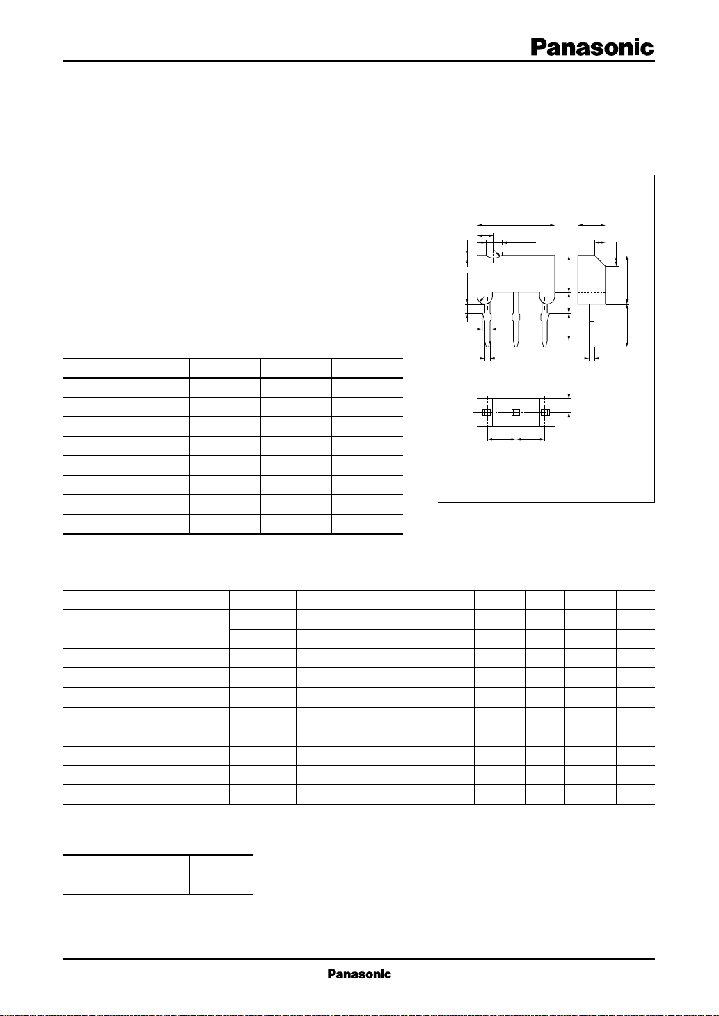
Absolute Maximum Ratings (Ta=25˚C)
■
Parameter
Collector to base voltage
Collector to emitter voltage
Emitter to base voltage
Peak collector current
Collector current
Collector power dissipation
Junction temperature
Storage temperature
Electrical Characteristics (Ta=25˚C)
■
Parameter
Collector cutoff current
Emitter cutoff current
Forward current transfer ratio
Transition frequency
Collector to emitter saturation voltage
Base to emitter voltage
Noise figure
Reverse transfer impedance
Common emitter reverse transfer capacitance
Symbol
V
CBO
V
CEO
V
EBO
I
CP
I
C
P
C
T
j
T
stg
Symbol
I
CBO
I
CEO
I
EBO
*
h
FE
f
T
V
CE(sat)
V
BE
NF
Z
rb
C
re
Ratings
–30
–20
–5
–60
–30
400
150
–55 ~ +150
.
CE(sat)
VCB = –10V, IE = 0
VCE = –20V, IB = 0
VEB = –5V, IC = 0
VCE = –10V, IC = –1mA
VCB = –10V, IE = 1mA, f = 200MHz
IC = –10mA, IB = –1mA
VCE = –10V, IC = –1mA
VCB = –10V, IE = 1mA, f = 5MHz
VCB = –10V, IE = 1mA, f = 2MHz
VCE = –10V, IC = –1mA, f = 10.7MHz
Unit
V
V
V
mA
mA
mW
˚C
˚C
Conditions
6.9±0.1
1.5
1.5 R0.9
0.4
R0.9
R0.7
1.0±0.1
0.85
0.55±0.1 0.45±0.05
2.5 2.5
1:Base
2:Collector EIAJ:SC–71
3:Emitter M Type Mold Package
min
typ
2.5±0.1
1.0
3.5±0.1
2.0±0.2
2.4±0.21.25±0.05
123
max
– 0.1
–100
–10
70
150
300
220
– 0.1
– 0.7
2.8
22
1.2
4.0
50
2.0
Unit: mm
1.0
4.1±0.2 4.5±0.1
Unit
µA
µA
µA
MHz
V
V
dB
Ω
pF
*
hFE Rank classification
Rank B C
h
FE
70 ~ 140 110 ~ 220
1
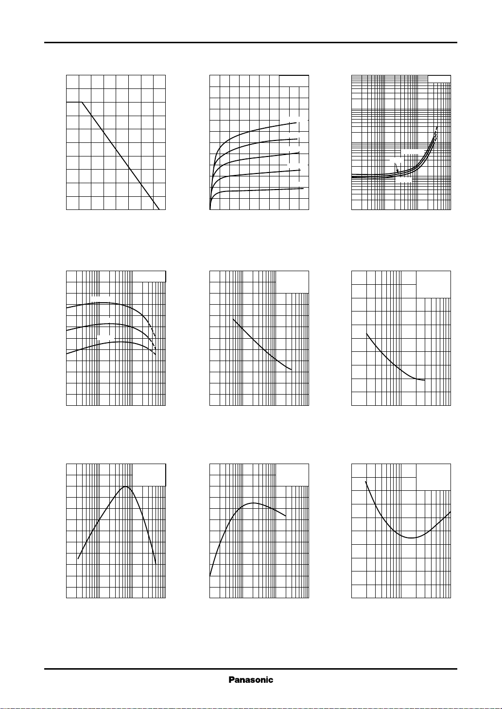
Transistor
2SA1254
PC—Ta IC—V
500
)
450
mW
(
400
C
350
300
250
200
150
100
50
Collector power dissipation P
0
0 16040 12080 14020 10060
Ambient temperature Ta (˚C
hFE—I
C
–120
FE
–100
–80
–60
–40
Ta=75˚C
25˚C
–25˚C
VCE=–10V
CE
)
–30
–25
)
mA
(
–20
C
–15
–10
Collector current I
–5
0
0 –10–8–2 –6–4
)
Collector to emitter voltage VCE (V
Cob—V
6
)
pF
(
5
ob
4
3
2
CB
Ta=25˚C
IB=–250µA
–200µA
–150µA
–100µA
–50µA
f=1MHz
I
=0
E
Ta=25˚C
–100
V
(
–30
CE(sat)
–10
–3
–1
– 0.3
– 0.1
– 0.03
– 0.01
Collector to emitter saturation voltage V
)
)
pF
(
re
V
CE(sat)—IC
IC/IB=10
Ta=75˚C
25˚C
–25˚C
– 0.1 –1 –10 –100– 0.3 –3 –30
Collector current IC (mA
Cre—V
5
4
3
2
CE
IC=–1mA
f=10.7MHz
Ta=25˚C
)
–20
Forward current transfer ratio h
0
– 0.1 –1 –10 –100– 0.3 –3 –30
Collector current IC (mA
fT—I
E
600
)
500
MHz
(
T
400
300
200
100
Transition frequency f
0
0.1 1 10 1000.3 3 30
VCB=–10V
Ta=25˚C
Emitter current IE (mA
1
1
Collector output capacitance C
0
– 0.1 –1 –10 –100– 0.3 –3 –30
)
Collector to base voltage VCB (V
PG—I
C
24
20
VCE=–10V
f=100MHz
Ta=25˚C
)
dB
(
16
12
8
Power gain PG
4
0
– 0.1 –1 –10 –100– 0.3 –3 –30
)
Collector current IC (mA
)
Common emitter reverse transfer capacitance C
0
–1 –3 –10 –30 –100
)
Collector to emitter voltage VCE (V
NF — I
E
5
4
)
dB
(
3
2
Noise figure NF
1
0
0.1 0.3 1 3 10
VCB=–10V
f=100MHz
Ta=25˚C
Emitter current IE (mA
)
)
2
 Loading...