

Panasonic 2SA0838 Datasheet
Transistor
2SA838
Silicon PNP epitaxial planer type
For high-frequency amplification
Complementary to 2SC1359
Features
■
●
High transition frequency fT.
Absolute Maximum Ratings (Ta=25˚C)
■
Parameter
Collector to base voltage
Collector to emitter voltage
Emitter to base voltage
Collector current
Collector power dissipation
Junction temperature
Storage temperature
Symbol
V
CBO
V
CEO
V
EBO
I
C
P
C
T
j
T
stg
Ratings
–30
–20
–5
–30
250
150
–55 ~ +150
Unit
V
V
V
mA
mW
˚C
˚C
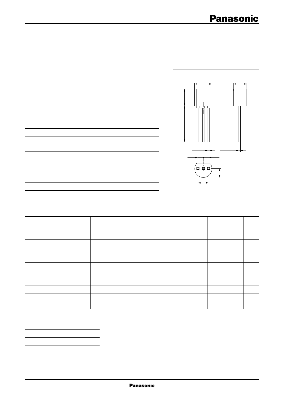
5.0±0.2 4.0±0.2
5.1±0.213.5±0.5
+0.2
0.45
–0.1
1.27 1.27
213
2.54±0.15
0.45
2.3±0.2
+0.2
–0.1
Unit: mm
1:Emitter
2:Collector
3:Base
JEDEC:TO–92
EIAJ:SC–43A
Electrical Characteristics (Ta=25˚C)
■
Parameter
Collector cutoff current
Emitter cutoff current
Forward current transfer ratio
Collector to emitter saturation voltage
Base to emitter voltage
Transition frequency
Noise figure
Reverse transfer impedance
Symbol
I
CBO
I
CEO
I
EBO
h
FE
V
CE(sat)
V
BE
f
T
NF
Z
rb
Common emitter reverse transfer
C
capacitance
*
hFE Rank classification
re
Rank B C
h
FE
70 ~ 140 110 ~ 220
Conditions
VCB = –10V, IE = 0
min
typ
max
– 0.1
Unit
µA
VCE = –20V, IB = 0
VEB = –5V, IC = 0
*
VCE = –10V, IC = –1mA
IC = –10mA, IB = –1mA
VCE = –10V, IC = –1mA
VCB = –10V, IE = 1mA, f = 200MHz
VCB = –10V, IE = 1mA, f = 5MHz
VCE = –10V, IC = –1mA, f = 2MHz
70
150
– 0.1
– 0.7
300
2.8
22
–100
–10
220
4.0
50
µA
V
V
MHz
dB
Ω
VCE = –10V, IC = –1mA,
1.2
2.0
pF
f = 10.7MHz
1
Transistor 2SA838
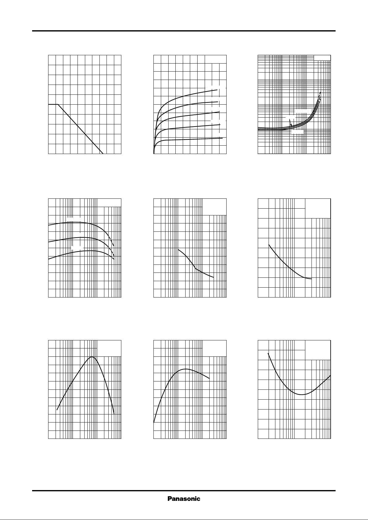
PC—Ta IC—V
500
)
450
mW
(
400
C
350
300
250
200
150
100
50
Collector power dissipation P
0
0 20016040 12080
Ambient temperature Ta (˚C
–120
FE
–100
hFE—I
Ta=75˚C
C
VCE=–10V
CE
)
–30
–25
)
mA
(
–20
C
–15
–10
Collector current I
–5
0
0 –10–8–2 –6–4
)
Collector to emitter voltage VCE (V
Cob—V
6
)
pF
(
5
ob
CB
Ta=25˚C
IB=–250µA
–200µA
–150µA
–100µA
–50µA
f=1MHz
I
=0
E
Ta=25˚C
–100
V
(
–30
CE(sat)
–10
–3
–1
– 0.3
– 0.1
– 0.03
– 0.01
Collector to emitter saturation voltage V
– 0.1 –1 –10 –100– 0.3 –3 –30
)
)
5
pF
(
re
4
V
CE(sat)—IC
IC/IB=10
Ta=75˚C
25˚C
–25˚C
Collector current IC (mA
Cre—V
CE
IC=–1mA
f=10.7MHz
Ta=25˚C
)
–80
–60
–40
–20
Forward current transfer ratio h
0
– 0.1 –1 –10 –100– 0.3 –3 –30
25˚C
–25˚C
Collector current IC (mA
fT—I
E
600
)
500
MHz
(
T
400
300
200
100
Transition frequency f
VCB=–10V
Ta=25˚C
4
3
3
2
2
1
1
Collector output capacitance C
0
– 0.1 –1 –10 –100– 0.3 –3 –30
)
Collector to base voltage VCB (V
PG — I
24
20
C
VCE=–10V
f=100MHz
Ta=25˚C
)
dB
(
16
12
8
Power gain PG
4
Common emitter reverse transfer capacitance C
0
–1 –3 –10 –30 –100
)
Collector to emitter voltage VCE (V
)
dB
(
NF — I
5
4
3
2
E
VCB=–10V
f=100MHz
Ta=25˚C
Noise figure NF
1
)
0
0.1 1 10 1000.3 3 30
Emitter current IE (mA
2
0
– 0.1 –1 –10 –100– 0.3 –3 –30
)
Collector current IC (mA
)
0
0.1 0.3 1 3 10
Emitter current IE (mA
)
 Loading...