

Panasonic 2SA0720, 2SA0719 Datasheet
Transistor
2SA719, 2SA720
Silicon PNP epitaxial planer type
For low-frequency power amplification and driver amplification
Complementary to 2SC1317 and 2SC1318
Features
■
●
Complementary pair with 2SC1317 and 2SC1318.
Absolute Maximum Ratings (Ta=25˚C)
■
Parameter
Collector to
base voltage
Collector to
emitter voltage
2SA719
2SA720
2SA719
2SA720
Emitter to base voltage
Peak collector current
Collector current
Collector power dissipation
Junction temperature
Storage temperature
Electrical Characteristics (Ta=25˚C)
■
Parameter
Collector cutoff current
Collector to base
voltage
Collector to emitter
voltage
Emitter to base voltage
Forward current transfer ratio
Collector to emitter saturation voltage
Base to emitter saturation voltage
Transition frequency
Collector output capacitance
2SA719
2SA720
2SA719
2SA720
Symbol
V
CBO
V
CEO
V
EBO
I
CP
I
C
P
C
T
j
T
stg
Symbol
I
CBO
V
CBO
V
CEO
V
EBO
*
h
FE1
h
FE2
V
CE(sat)
V
BE(sat)
f
T
C
ob
Ratings
–30
–60
–25
–50
–5
–1
–500
625
150
–55 ~ +150
Unit
V
V
V
A
mA
mW
˚C
˚C
Conditions
VCB = –20V, IE = 0
IC = –10µA, IE = 0
IC = –10mA, IB = 0
IE = –10µA, IC = 0
VCE = –10V, IC = –150mA
VCE = –10V, IC = –500mA
IC = –300mA, IB = –30mA
IC = –300mA, IB = –30mA
VCB = –10V, IE = 50mA, f = 200MHz
VCB = –10V, IE = 0, f = 1MHz
5.0±0.2 4.0±0.2
5.1±0.213.5±0.5
+0.2
0.45
–0.1
1.27 1.27
213
2.54±0.15
min
typ
–30
–60
–25
–50
–5
85
40
– 0.35
–1.1
200
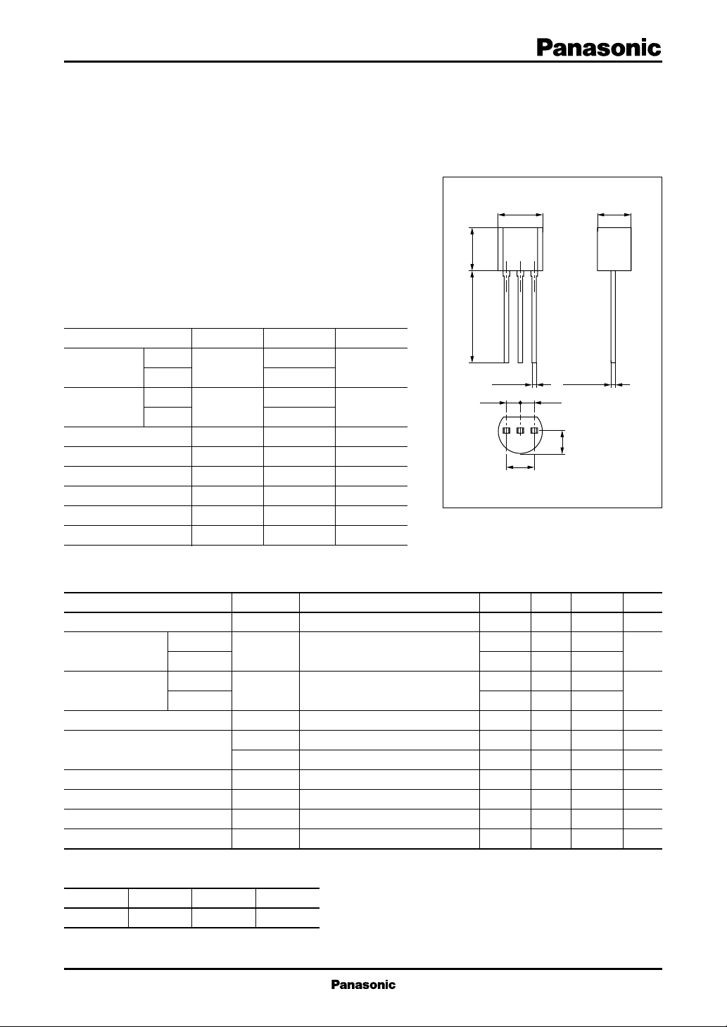
Unit: mm
+0.2
0.45
–0.1
1:Emitter
2.3±0.2
2:Collector
3:Base
JEDEC:TO–92
EIAJ:SC–43A
max
– 0.1
Unit
µA
V
V
V
340
– 0.6
–1.5
V
V
MHz
6
15
pF
*
h
Rank classification
FE1
Rank Q R S
h
FE1
85 ~ 170 120 ~ 240 170 ~ 340
1
Transistor 2SA719, 2SA720
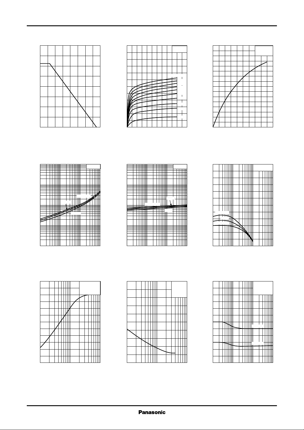
PC—Ta IC—V
800
)
700
mW
(
C
600
500
400
300
200
100
Collector power dissipation P
0
0 16040 12080 14020 10060
Ambient temperature Ta (˚C
V
CE(sat)—IC
)
–10
V
(
–3
CE(sat)
–1
– 0.3
– 0.1
– 0.03
– 0.01
– 0.003
– 0.001
Collector to emitter saturation voltage V
–1 –10 –100 –1000–3 –30 –300
Ta=75˚C
25˚C
–25˚C
Collector current IC (mA
)
IC/IB=10
)
CE
12
10
)
mA
(
8
C
6
4
Collector current I
2
0
012108264
Ta=25˚C
IB=–1.0mA
– 0.9mA
– 0.8mA
– 0.7mA
– 0.6mA
– 0.5mA
– 0.4mA
– 0.3mA
– 0.2mA
– 0.1mA
Collector to emitter voltage VCE (V
V
BE(sat)—IC
–100
)
V
(
–30
BE(sat)
–10
–3
–1
– 0.3
– 0.1
– 0.03
Base to emitter saturation voltage V
– 0.01
–1 –10 –100 –1000–3 –30 –300
Ta=–25˚C
IC/IB=10
25˚C
75˚C
Collector current IC (mA
IC—I
B
–800
–700
)
–600
mA
(
C
–500
–400
–300
–200
Collector current I
–100
0
0 –10–8–2 –6–4
)
Base current IB (mA
hFE—I
600
FE
500
400
300
Ta=75˚C
25˚C
200
–25˚C
100
Forward current transfer ratio h
0
– 0.01
)
– 0.1 –1 –10
– 0.03
Collector current IC (A
VCE=–10V
Ta=25˚C
C
VCE=–10V
– 0.3 –3
)
)
fT—I
240
)
200
MHz
(
T
160
120
80
40
Transition frequency f
0
1 3 10 30 100
Emitter current IE (mA
2
E
VCB=–10V
Ta=25˚C
)
Cob—V
50
)
45
pF
(
40
ob
35
30
25
20
15
10
5
Collector output capacitance C
0
–1 –3 –10 –30 –100
CB
Collector to base voltage VCB (V
IE=0
f=1MHz
Ta=25˚C
–120
)
V
(
–100
CER
–80
–60
–40
–20
Collector to emitter voltage V
0
1 10 100 10003 30 300
)
Base to emitter resistance RBE (kΩ
V
CER—RBE
IC=–2mA
Ta=25˚C
2SA720
2SA719
)
 Loading...