

Page 1

Prevention of Electrostatic Discharge (ESD) to Electrostatically
Sensitive (ES) Devices
Some semiconductor (solid state) devices can be damaged easily by static electricity. Such components commonly are
called Electrostatically Sensitive (ES) Devices. Examples of typical ES devices are integr ated circuits and some field-effect
transistors and semiconductor "chip" components. The following techniques should be used to help reduce the incidence of
component damage caused by electrostatic discharge (ESD).
1. Immediately before handling any semiconductor component or semiconductor-equipped assembly, drain off any ESD on
your body by touching a known earth ground. Alternatively, obtain and wear a commercially available discharging ESD
wrist strap, which should be removed for potential shock reasons prior to applying power to the unit under test.
2. After removing an electrical assembly equipped with ES devices, place the assembly on a cond uctive surface such as
aluminum foil, to prevent electrostatic charge build up or exposure of the assembly.
3. Use only a grounded-tip soldering iron to solder or unsolder ES devices.
4. Use only an anti-static solder removal device. Some solder removal devices not classified as "anti-static (ESD
protected)" can generate electrical charge sufficient to damage ES devices.
5. Do not use freon-propelled chemicals. These can generate electrical charges sufficient to damage ES devices.
6. Do not remove a replacement ES device from its protective package until immediately before you are ready to install it.
(Most replacement ES devices are packaged with leads electrically shorted together by cond uctive foam, aluminum foil
or comparable conductive material).
7. Immediately before removing the protective material from the leads of a replacement ES device, touch the protective
material to the chassis or circuit assembly into which the device will be installed.
Caution
Be sure no power is applied to the chassis or circuit, and observe all other safety precautions.
8. Minimize bodily motions when handling unpackaged replacement ES devices. (Otherwise harmless motion such as th e
brushing together of your clothes fabric or the lifting of your foot from a carpeted floor can generate static electricity
(ESD) sufficient to damage an ES device).
There are special components used in this equipment which are important for safety.
These parts are marked by in schematic diagrams, exploded views and replacement parts list. It is essential that
these critical parts should be replaced with manufacturer’s specified parts to prevent shock, fire, or other hazards. Do
not modify the original design without permission of manufacturer.
IMPORTANT SAFETY NOTICE
Page 2
About lead free solder (PbF)
Note: Lead is listed as (Pb) in the periodic table of elements.
In the information below, Pb will refer to Lead solder, and PbF will refer to Lead Free Solder.
The Lead Free Solder used in our manufacturing process and discussed below is (Sn+Ag+Cu).
That is Tin (Sn), Silver (Ag) and Copper (Cu) although other types are available.
This model uses Pb Free solder in it’s manufacture due to environmental conservation issues. For service and repair work,
we’d suggest the use of Pb free solder as well, although Pb solder may be used.
PCBs manufactured using lead free solder will have the PbF within a leaf Symbol
stamped on the back of PCB.
Caution
Pb free solder has a higher melting point than standard solder. Typically the melting point is 50 ~ 70 °F (30~40°C)
higher. Please use a high temperature soldering iron and set it to 700 ± 20 °F (370 ± 10 °C).
Pb free solder will tend to splash when heated too high (about 1100 °F or 600 °C).
If you must use Pb solder, please completely remove all of the Pb free solder on the pins or solder area before
applying Pb solder. If this is not practical, be sure to heat the Pb free solder until it melts, before applying Pb solder.
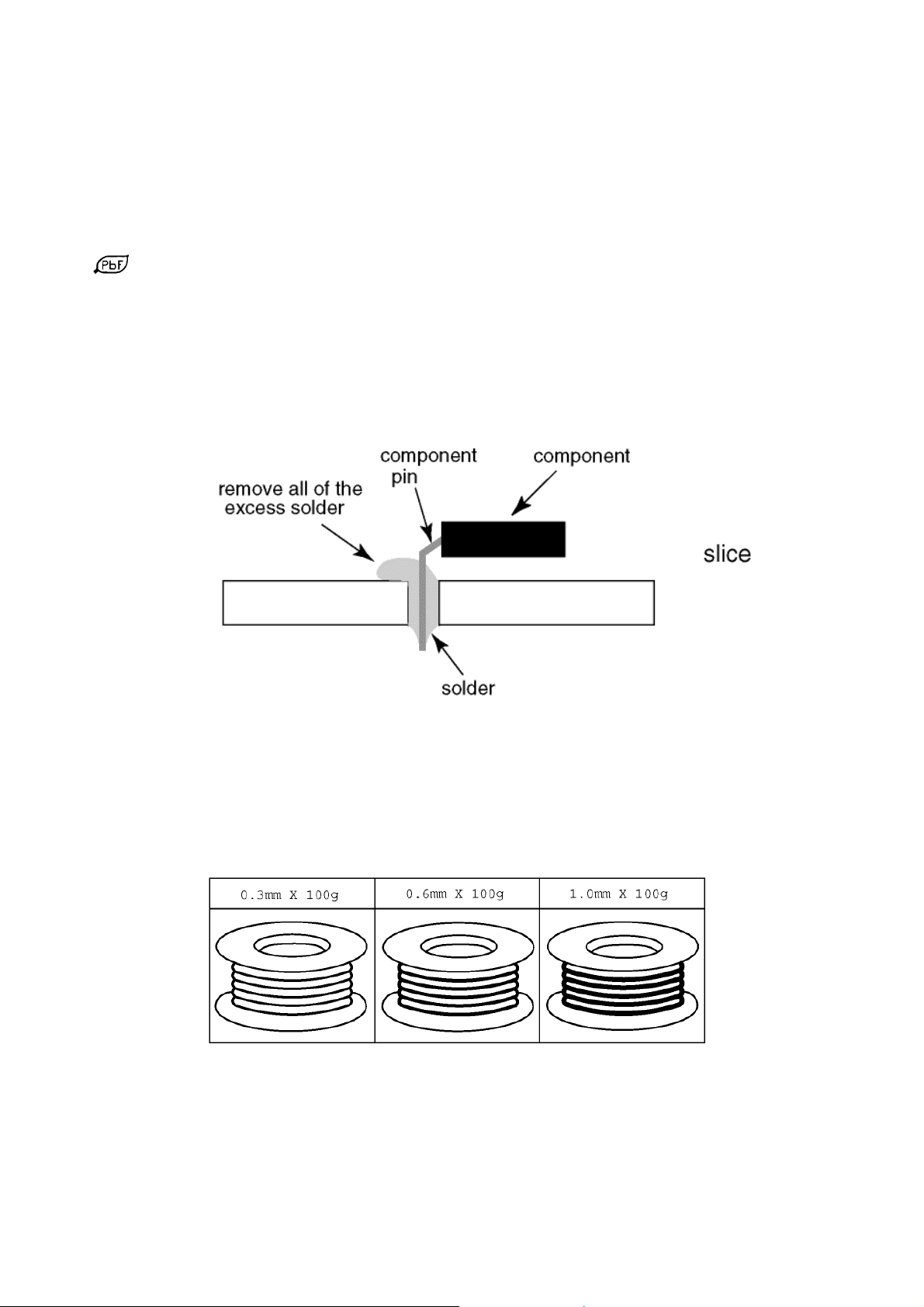
After applying PbF solder to double layered boards, please check the com ponent side for excess solder which may
flow onto the opposite side. (see Fig.3)
Suggested Pb free solder
There are several kinds of Pb free solder available for purchase. This product uses Sn+Ag+Cu (tin, silver, copper) solder.
However, Sn+Cu (tin, copper), Sn+Zn+Bi (tin, zinc, bismuth) solder can also be used. (see Fig.4)
Fig.3
Fig.4
 Loading...