

PAN MULTILAYER CERAMIC CAPACITOR Specification
Document No.: M01-00-E-03
PRODUCT: MULTILAYER CERAMIC CAPACITOR
TYPE : CHIP CAPACITOR
APPROVED BY CUSTOMER
PAN OVERSEAS ELECTRONIC CO., LTD.
TAIWAN HEAD OFFICE:
TEL: 02-25213252~5, 02-25634133
FAX: 02-25373069
TAIWAN FACTORY:
TEL: 06-6982143, 06-6982331
FAX: 06-6983400,(QA:06-6993898)
PAN OVERSEAS
PAN OVERSEAS (GUANG ZHOU):
TEL: 86-20-82237476
FAX: 86-20-82237475
PAN OVERSEAS (KUN SHAN):
TEL: 86-512-57707888
FAX: 86-512-57711076
QUALITY ASSURANCE DEPARTMENT
APPROVED
▓
TAIWAN
CHECKED
□
GUANG ZHOU□KUN SHAN
PREPARED
PAN OVERSEAS ELECTRONIC CO., LTD
M01-00-E-03
SPECIFICATION OF MULTILAYER CERAMIC CHIP CAPACITOR
Ver: 3
Code
voltage
Code
voltage
Code
voltage
Code
voltage
Code
voltage
6.3V
200V
630V
3000V
10V
250V
1000V
4000V
16V
100V
500V
2000V
5000V
Length (L)
Width (W)
Thickness (T)
MB(Min)
G(Min)
6.3~ 50V
6.3~250V
6.3~500V
10.16±0.5
15.24±0.5
1. SCOPE
This specification is applicable to Pan Overseas multilayer ceramic capacitors.
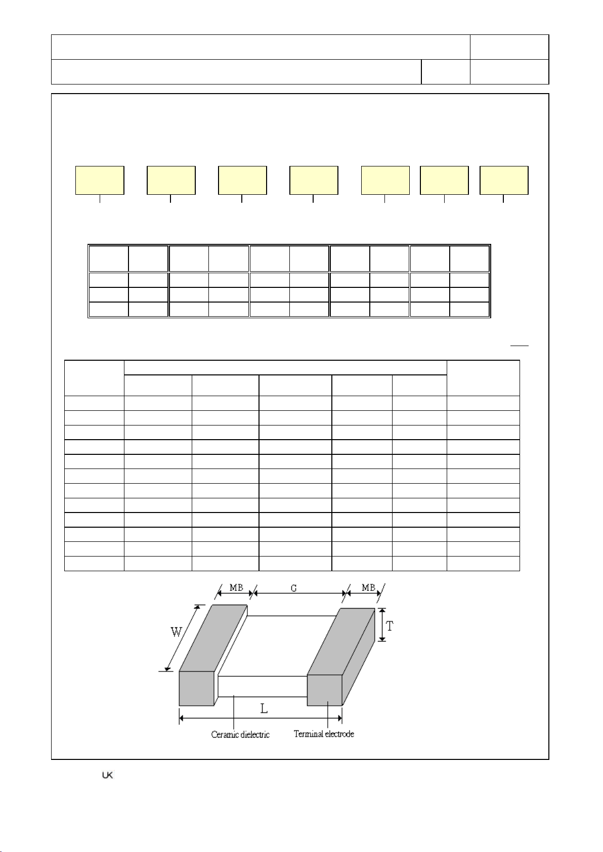
2.CODE CONSTRUCTION
U 0805 C
:
102
J N T
À Á Â Ã Ä Å Æ
À Rated Voltage:
K
N
B
Rated
T 25V G
U 50V H
A
Rated
C
Rated
D
M
M2
Rated
M3
M4
M5
Á Part Dimension:
Dimension
Page: 1
Rated
Unit: mm
0402 1.0±0.05 0.5±0.05 0.5±0.05 0.10 0.30
0603 1.6±0.1 0.8±0.1 0.8±0.1 0.20 0.40
0805 2.0±0.2 1.25±0.1 1.40 max. 0.25 0.70
1206 3.2±0.2 1.60±0.2 1.52 max. 0.25 1.40 6.3~1KV
1210 3.2±0.3 2.5±0.3 1.8 max. 0.25 1.40 6.3~1KV
1808 4.5±0.35 2.0±0.3 2.0 max. 0.25 2.15 6.3~5KV
1812 4.5±0.35 3.2±0.3 1.8 max. 0.25 2.15 16~5KV
2220 5.7±0.4 5.0±0.4 1.8 max. 0.25 3.30 16~5KV
2225 5.7±0.4 6.3±0.4 1.8 max. 0.25 3.30 16~5KV
3640 9.2±0.5
2.0 max. 0.50 2.70 16~5KV
5550 14.0±0.5 12.7±0.5 2.5 max. 0.50 10.5 16~5KV
8060 20.3±0.5
2.5 max. 0.50 16.8 16~5KV
PAN OVERSEAS
PAN OVERSEAS ELECTRONIC CO., LTD
M01-00-E-03
SPECIFICATION OF MULTILAYER CERAMIC CHIP CAPACITOR
Ver: 3
M Tolerance
Z Tolerance
and RH 45 to 75%.
If any doubt and argument has been encounter in judgement, the final test shall be done at 25±2
+80% / -20%
Code
Capacitance(pF)
Code
Capacitance(pF)
102
1R5
222
472
103
+125
+125
+85
+85
-82%
+85
-56%
 Temperature Characteristics Code:
Code Temp. Coefficient Operation Temp. Capacitance Change
C NP0 (Class I)
R X7R (Class II)
X X5R (Class II)
F Y5V (Class II)
E Z5U (Class II)
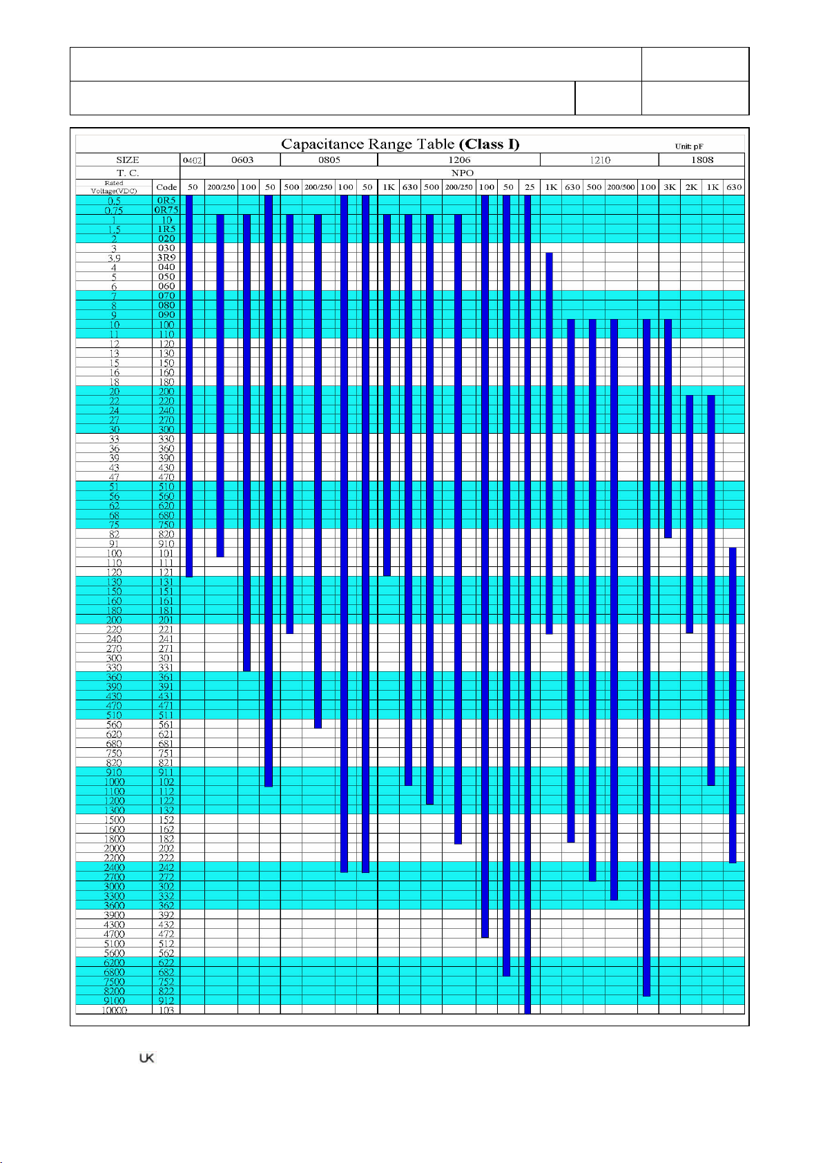
à Capacitance Code:
010 1 *
1.5
100 10 *
101 100 *
-55℃ ~
-55℃ ~
-55℃ ~
-30℃ ~
+10℃ ~
1000 *
2200 *
4700 *
10000 *
℃ 0 ± 30 ppm/℃
℃
℃
± 15%
± 15%
℃ +22% ~
℃ +22% ~
Ä Tolerance Code:
Code Tolerance Code Tolerance
B ± 0.1pF J ±5%
C ±0.25pF K ±10%
D ±0.50pF M ±20%
F ± 1% Z
G ± 2%
Page: 2
PS: 1. * -- Two significant digits followed by no. of zeros
2. Temperature coefficient (T.C.) vs. Proper tolerance applied:
NPO: For all tolerance
X7R、X5R: K、
Y5V、Z5U: M、
Å Termination Code:
Code N
Termination Type Nickel
3. STANDARD TEST CONDITIONS
:
Æ Packaging Code:
Code B T
Packaging Type Bulk Tape & Reel
Tests shall, unless otherwise specified, be carried out at 15 to 35℃
℃,RH45 to 55% and 860~1060mbar. (Based on JIS standard)
4. DISPOSITION
If question to the measuring result in judgement, take the capacitor under a specified temperature
for 30 minutes at least before measurement.
PAN OVERSEAS
PAN OVERSEAS ELECTRONIC CO., LTD
M01-00-E-03
SPECIFICATION OF MULTILAYER CERAMIC CHIP CAPACITOR
Ver: 3
Cu layer
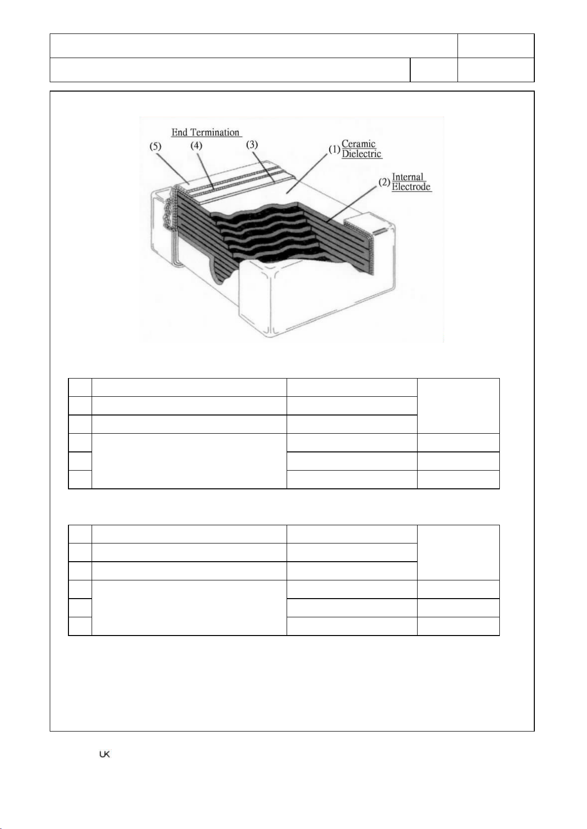
5. STRUCTURE:
Page: 3
Ag / Pd SERIES:
NO Specifications Material
1 Ceramic dielectric Ceramic
2 Internal Electrode Ag-Pd
Termination
Plating
thickness
3 Ag layer 40μm min
4 Ni layer 1.5-3.5μm min
5
End Terminal
Sn-Pb layer or Sn layer 3-8μm min
BME SERIES:
NO Specifications Material
1 Ceramic dielectric Ceramic
2 Internal Electrode Ni
3
4 Ni layer 1.5-3.5μm min
5
End Termination
Sn-Pb layer or Sn layer 3-8μm min
Termination
Plating
thickness
40μm min
6. STORING CONDITION AND TERM
Recommends the storing of products within 6 months at temperature 15~35℃ and humidity
70%RH max. If the product stored over 6 months, please reconfirm its solderability before use.
PAN OVERSEAS
PAN OVERSEAS ELECTRONIC CO., LTD
M01-00-E-03
SPECIFICATION OF MULTILAYER CERAMIC CHIP CAPACITOR
Ver: 3
Visual inspection & Dimension
Apply DC tested voltage for 60
< 30pF :
。
Page: 4
7. PERFORMANCE:
NO. Item Performance Test or Inspection method
(1) External
Appearance
Voltage Proof Withstand test voltage without
(2)
No defects which may affect
performance.
Insulation breakdown or other
damage.
measurement
DC Tested voltage shall be applied for
1~5sec. Charge/discharge current
shall not exceed 50 mA .
(PS: Ra – Rated Voltage )
Rated
voltage
DC Tested voltage
NPO X7R/X5R Y5V
≦200V 2.5Ra
250V 2.0Ra
500V/630V 1.5Ra
Insulation
(3)
Resistance
(4) Capacitance
(Cap.)
(5) Dissipation
Factor (D. F.)
NPO:
100,000MΩ Min. or
R‧C ≧ 1,000 Ω.F
(Whichever is smaller)
X7R, X5R, Y5V, Z5U:
10,000MΩ Min or
R‧C ≧ 1,000Ω.F
(Whichever is smaller)
Within the specified tolerance that
refers on page 2
NPO:
≧30pF: Q ≧ 1000
Q≧400+20C
PS: C: Nominal Capacitance (pF)
X7R、X5R、Y5V& Z5U:(Max. value)
T.C.≧50V 25V 16V
X7R/
X5R
Z5U 4.0% --- --- ---
Y5V 5.0% 7.5% 9.0% 12.5%
2.5% 3.0% 3.5% 5.0%
≦
10V
≧1K
V 1.5Ra 1.25Ra -----
±5
minute.
(PS: Ra – Rated Voltage)
Rated voltage
DC Tested voltage
<1KV 1.0 Ra
≧1KV 1KV
Measuring frequency:
Z5U、Y5V、X7R、X5R:1KHz±50Hz
NPO:>1000pF:1KHz±50Hz。
≦1000pF:1MHz±100KHz
Measuring voltage:
Z5U:0.5 Vrms
NPO、X7R、X5R、Y5V:1.0±0.2 Vrms
PAN OVERSEAS
PAN OVERSEAS ELECTRONIC CO., LTD
M01-00-E-03
SPECIFICATION OF MULTILAYER CERAMIC CHIP CAPACITOR
Ver: 3
The temperature coefficient is
determined using the capacitance
measured in step 3 as a reference.
Test the specimen from step 1
through step 5, the capacitance shall
be within the specified tolerance for
the capacitance coefficient and
Temperature(℃)
NPO
X7R
X5R
Y5V
Z5U
-55~+125
-55~+125
0±30(ppm/℃)
+22%~ -56%
Completely soak both terminal electrodes in
a. For Tin-Lead Sn/Pb) Termination product:
b. For Lead-free (Pure Sn) Termination
Completely soak both terminal
electrodes in solder at 270±5℃ for
appearance
C<30pF:Q≧400+20*C
(Max. value)
for
Leave the capacitors in ambient
condition for
hours before
Page: 5
NO. Item Performance Test or Inspection method
(6) Temperature
Characteristic of
Temperatures Coefficient
Operating Capacitance
T.C.
Capacitance
Temperature Change(ΔC)
℃
℃
-55~+85℃
-30~+85℃
± 15%
± 15%
+22%~-
82%
+10~+85℃
capacitance change as left table.
Step
1 Base Temp.(25℃)±2℃
2 Min. Operation Temp.±2℃
3 Base Temp.(25℃)±2℃
4 Max. Operation Temp.±2℃
5 Base Temp.(25℃)±2℃
(7) Solderability
New solder to over 95% of
termination
solder at specified temperature for 3±0.5 sec.:
235±5℃
(8) Leaching
(9) Solder-
ing to
Heat
External
Cap. change
(ΔC/C)
D.F.
I.R.
New solder to over 95% of
termination
No mechanical damage.
NPO
X7R/X5R
Z5U
Y5V
±2.5% or ± 0.25 pF max.
( Whichever is larger)
±7.5%
±20%
±20%
NPO: C≧30pF:Q≧1000
PS: C: Nominal Capacitance (pF)
X7R、X5R、Y5V& Z5U:
T.C.≧50V 25V 16V
X7R/
X5R
Z5U 4.0% --- --- ---
Y5V 5.0% 7.5% 9.0% 12.5%
NPO:
X7R、X5R、Y5V、Z5U:
2.5% 3.0% 3.5% 5.0%
100,000MΩ Min. or
R‧C ≧ 1,000 Ω.F
(Whichever is smaller)
10,000MΩ Min or
R‧C ≧ 1,000Ω.F
(Whichever is smaller)
≦
10V
product: 245±5℃
40±1 sec.
Completely immerse both
terminations in solder at 270±5℃
10±3 sec.
24±2
measurement.
*Preconditioning:(only for Class 2):
Perform a heat treatment at 150 +0-
10℃ for one hour and then let sit for
24 ± 2 hours at room temperature.
Perform the initial measurement.
PAN OVERSEAS
PAN OVERSEAS ELECTRONIC CO., LTD
M01-00-E-03
SPECIFICATION OF MULTILAYER CERAMIC CHIP CAPACITOR
Ver: 3
PS: C: Nominal Capacitance
X7R/ X5R: Less than 2 times
Y5V & Z5U: Less than 1.5
min. or 25
A. Humidity load: (Not apply for the
product with rated voltage
Apply the rated voltage at
temperature 40±2℃ and humidity
90 to 95%RH for 1000+48/-0
Leave the capacitors in ambient
condition for the following time
* Charge / discharge current shall. not
* Preconditioning:(only for Class 2):
Apply the
(Whichever is larger
PS: C: Nominal Capacitance
X7R/ X5R: Less than 2 times
Y5V & Z5U: Less than 1.5
Page: 6
NO. Item Performance Test or Inspection method
(10)
Humidity
(Steady
state)
&
Humidity
load
External
appearance
Cap. change
(ΔC/C)
D.F.
No mechanical damage.
NPO: ± 5% or ±0.5 pFmax.
(Whichever is larger)
X7R/
X5R:±
12.5
﹪
Y5V: ±30%
Z5U: ±30%
NPO:
C≧30pF: Q ≧350
10pF≦C<30pF:
250V):
hours.
before measurement.
Class 1:1~2 hours.
Class 2:24±2hours.
Q≧100+2.5*C
C<10pF: 200+10*C
(pF)
exceed 50 mA.
rated DC voltage for 1hour
at 40±2℃. Remove and let sit for
of initial value
48±4 hours at room temperature.
Perform initial measurement.
≧
(11) Load Life
I.R.
External
appearance
Cap. change
(ΔC/C)
D.F.
I.R.
times of initial value
500MΩ
(Whichever is smaller)
Ω*F
No mechanical damage.
NPO: ±3% or ±0.3pFmax.
X7R/
X5R:±
12.5
﹪
Y5V: ±30%
Z5U: ±30%
NPO:
C≧30pF: Q≧350
30pF>C≧10pF:
Q≧275+2.5*C
C<10pF:Q≧200+10*C
(pF)
of initial value
times of initial value
1000MΩ min. or 50Ω*F
(Whichever is smaller)
B. Humidity (Steady state):
The test procedure is same as that
in Humidity load but only without
rated voltage applied.
Apply 2×rated voltage at maximum
operating temperature ±2℃ for 1000
+48/-0 hours.
)
Leave the capacitors in ambient
condition for the following time
before measurement.
Class I: 1~2 hours
Class II: 24±2 hours
* Charge / discharge current shall. not
exceed 50 mA.
* Preconditioning:(only for Class 2):
Apply 200% of the rated DC voltage
for 1 hour at the maximum operating
temperature ± 3℃. Remove and let sit
for 24±2 hours at room temperature.
Perform initial measurement.
PAN OVERSEAS
PAN OVERSEAS ELECTRONIC CO., LTD
M01-00-E-03
SPECIFICATION OF MULTILAYER CERAMIC CHIP CAPACITOR
Ver: 3
(Whichever is larger
PS: C: Nominal Capacitance
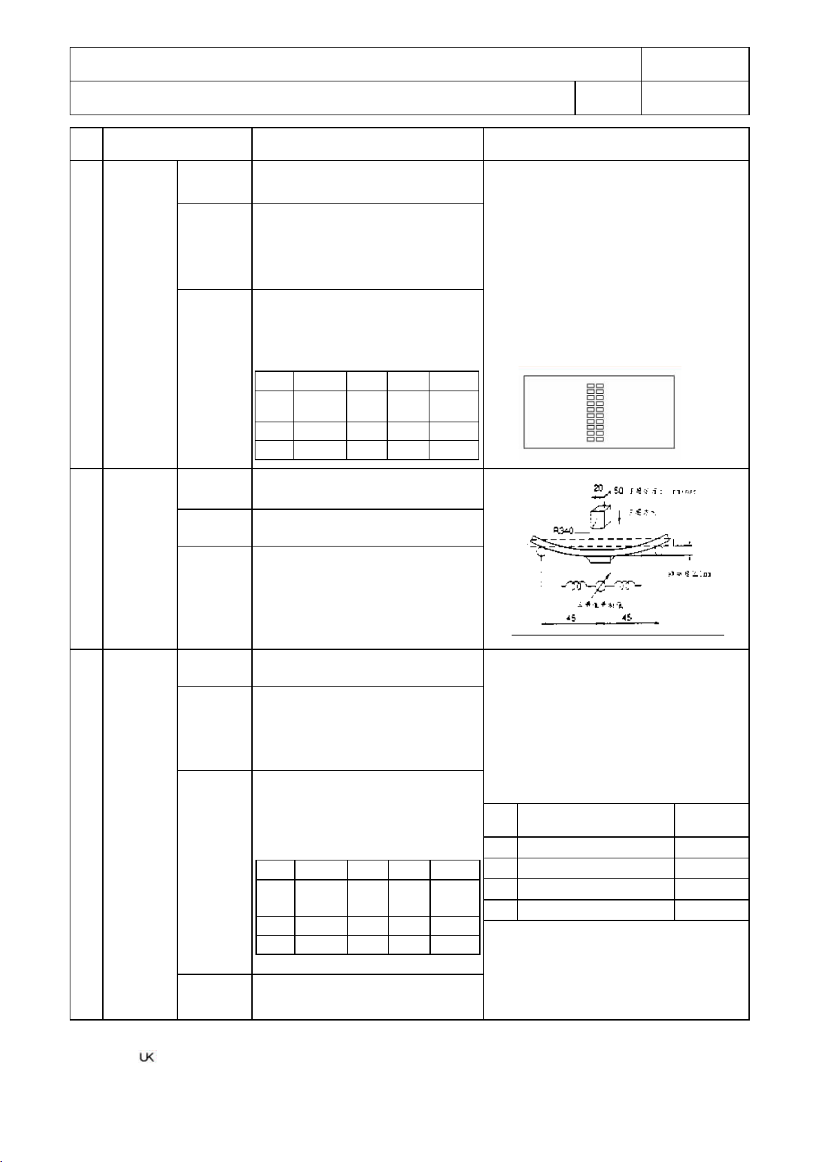
Solder the capacitors to the test jig as shown
in figure below with IR-Reflow method. The
capacitor shall be subjected to a simple
harmonic motion with the entire frequency
range, from 10 to 55 Hz and return to 10
Amplitude(total excursion):1.5mm
Amplitude tolerance:
This motion shall be applied for a period of 2
hours in each of 3 mutually perpendicular
appearance
appearance
The capacitor shall be subject 5 cycles
according to four heat treatments
Then Leave the capacitors in ambient
condition for the following time
Step
Duration
(min.)
1
2
3
4
min. or 500
*Preconditioning:(only for Class 2):
Perform a heat treatment at 150
+0-10
X5R
Page: 7
NO. Item Performance Test or Inspection method
(12)Vibration
(13)Deflectio
External
appearance
Cap.
change
(ΔC/C)
D.F. or Q
External
Without distinct damage
NPO: ±2.5% or ±0.25pF max.
)
X7R
/ X5R:±
Y5V、Z5U: ±
NPO: C≧30pF:Q≧1000
C<30pF:Q≧400+20*C
X7R、X5R、Y5V& Z5U:(Max. value)
T.C.≧50V 25V 16V
X7R/
Z5U 4.0% --- --- ---
Y5V 5.0% 7.5% 9.0% 12.5%
2.5% 3.0% 3.5% 5.0%
7.5
20%
﹪
(pF)
≦
No cracking or marking defects
(Not apply for 0402 product)
Hz ,shall be transverse in 1 min.
directions (a total of 6 hours)
10V
±15%
shall occur
n
Bending
Flexure ≧ 1mm
strength
Cap.
change
(ΔC/C)
NPO: ±5% or±0.5pFmax.
( Whichever is larger)
X7R
/ X5R
: ±12.5﹪
Y5V: ±30﹪
(14
Temperatur
)
e cycle
PAN OVERSEAS
External
Cap.
change
(ΔC/C)
D.F.
I.R.
No mechanical damage.
NPO: ±2.5% or ±0.25pFmax.
( Whichever is larger)
X7R
/ X5R:±
7.5
﹪
Y5V: ±20﹪
NPO:
C≧30pF:Q≧1000
C<30pF:Q≧400+20*C
X7R、X5R Y5V&Z5U: (Max. value)
T.C.≧50V 25V 16V
X7R/
X5R
Z5U 4.0% --- --- ---
Y5V 5.0% 7.5% 9.0% 12.5%
2.5% 3.0% 3.5% 5.0%
10000MΩ
(Whichever is smaller)
≦
Ω*F
10V
(Not apply for 0402 product)
listed in the following table.
before measurement.
Class II: 2 ~ 24 hours
Temperature (℃)
Min. Operation Temp.±3 30±3
Room Temp. (25℃) 2 ~ 5
Max. Operation Temp.±3 30±3
Room Temp. (25℃) 2 ~ 5
℃ for one hour and then let sit
for 24±2 hours at room temperature.
Perform the initial measurement.
PAN OVERSEAS ELECTRONIC CO., LTD
M01-00-E-03
SPECIFICATION OF MULTILAYER CERAMIC CHIP CAPACITOR
Ver: 3
Page: 8
PAN OVERSEAS
 Loading...