

Page 1
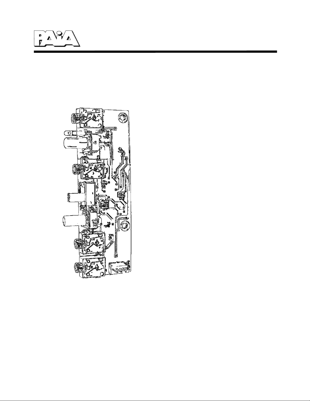
Sample and Hold
Model 9752
Assembly and Using Manual
This second-generation 9700-series processing
element for modular sound synthesizers is
designed to provide great sound and excellent
value.
The 9752 monitors the input signal voltage and
copies it to the output, synchronized to changes in
an input control voltage (CV) or an input clock, or
synchronized to an internal clock if there is no
external input. The input may be an audio or
control signal. One typical application uses noise
as an input signal and a variable rate clock to
control sampling. This provides a random control
voltage source from the module output.
The module's use with audio signals is enhanced
by a switch option to change the function from
"sample and hold" to "gate and hold", where the
output tracks the input signal as long as the
control input voltage is above a threshold (or, if
selected, the internal clock rises). After the control
voltage drops, the output voltage freezes until the
next high-going transition of the control voltage (or
the internal clock rises again).
© 2009 PAiA Corporation
This high-performance module is designed to be
compatible with most modular synthesizer
systems with little or no modification. Most active
components are already mounted, making
assembly a snap.
Page 2

ASSEMBLING THE 9752 Sample and Hold
Before beginning assembly, go through the manual. Look at the drawings.
Feel the parts. You're naturally eager to plunge right in, but take a few
deep breaths first. Check the parts supplied against the packing list at the
back of this manual.
In some cases, notes packed with the parts will be used to call your attention
to special situations. If parts are missing, please notify PAiA at
[email protected] or by phone at (405) 340-6300, fax (405) 340-6378. A
NOTES page is included at the end of this manual.
Notice that each step in the manual is marked with a
checkoff box like this:
DESIGNATION DESC. MARKING
( ) R27 100ohm brn-blk-brn-gld
Checking off each step as you do it may seem silly and ritualistic, but it
greatly decreases the chance of omitting a step and also provides some
gratification and reward as each step is completed.
Numbered figures are printed in the Illustrations Supplement in the center of
this manual. These pages may be removed for easy reference during
assembly.
THE CIRCUIT BOARD
The 9752 Sample and Hold is built on a double-sided circuit board. Note the
“top” side of the board has the connector and control placement designators.
Surface-mounted components are on the “bottom” of the board. Install parts
to the top of the board and solder them on the bottom.
TOOLS
You'll need a minimum of tools to assemble the kit – a small pair of diagonal
wire cutters, pliers, screwdriver, soldering iron, and solder.
2
Page 3

Modern electronic components are small (in case you hadn't noticed) and
values marked on the part are often difficult to see. Another handy tool for
your bench will be a good magnifying glass. Also use the magnifier to
examine each solder joint as it is made to make sure that is doesn't have
any of the problems in the SOLDERING section which follows.
SOLDERING
Select a soldering iron with a small tip and a power rating of not more than
35 watts. Soldering guns are completely unacceptable for assembling
solid-state equipment because the large magnetic field they generate can
damage components.
Use only a high quality electronic solder. Your kit is compatible with leadfree and/or tin-lead flux-core solders made especially for electronic
assembly. Plumbing solder will destroy your kit with its acid core. Jewelry
solder (silver solder) will destroy your kit with its high working heat. Neither
is for electronics work.
A proper solder joint has just enough solder to cover the soldering pad and
about 1/16-inch of the lead passing through it.
There are two improper connections to be aware of: Using too little solder
will sometimes result in a connection which appears to be soldered when
actually there is a thin layer of flux insulating the component lead from the
solder bead. This situation can be cured by reheating the joint and applying
more solder.
Too much solder may produce a conducting bridge of excess solder
between adjacent pads causing a short-circuit. Continued feeding of solder
into a hot joint can result in accumulation on the underside of the board and
may cause bridges or impede the action of mechanical components. If you
see this, position the board above the iron tip and the excess will flow to the
tip.
Use care when mounting all components. Never force a component into
place.
3
Page 4
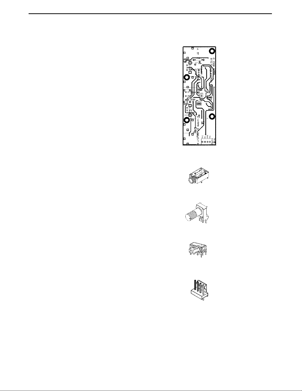
CONTROLS AND CONNECTORS
Controls and connectors will be installed on the top
side of the board with the placement designators as
shown in the illustration to the right.
Miniature phone connectors referenced as “stereo
phone jacks” in the manual parts list are specified
below with the contact/terminal names, Tip, Ring and
Sleeve (TRS) and are labeled on the board and
schematic as such.
The potentiometers have tabs extending from their body
for stability. They have a snap-fit to the board. Align
the tabs and pins with their holes and press them into
place. There is no need to bend the tabs or terminals.
To ensure the best alignment with these parts with the
front panel, begin by soldering only one of the multiple
terminals associated with each of the following parts
as it is installed. Then, if a part is tilted or crooked, it
is only a matter of reheating the joint as the part is
aligned.
Match the tab of the polarized power connector with the
corresponding board marking.
Top of circuit board
DESIG. DESC. MARKING
( ) J1 TRS socket, c.c. 4 terminals
( ) J2 TRS socket 3 terminals
( ) J3 TRS socket 3 terminals
( ) J4 TRS socket 3 terminals
( ) P1 100K ohm B100K
potentiometer, linear
( ) P2 1M ohm A1M
potentiometer, audio
( ) SW1 Slide Switch
( ) PWR1 Header
TRS socket
“stereo phone jack”
Potentiometer
Slide Switch
Header
4
Page 5

CAPACITORS
Install the non-polarized polyester capacitor. Either lead can go
in either hole. Locations are provided for optional, time constant
altering capacitors at the Cs 12, 13 and 15 designations.
Do not install these parts for standard applications.
( ) C3 0.01uF 103, 10n, 10n6J3
RESISTORS
There is a designation for a fixed resistor, R16, on the board:
however, it is an option made available for instances in which
a substitution is made for the indicator LED. Do not install a
part here for standard applications.
LED
The legs of the LED will be bent at a right angle so when
it is installed, it will project through a hole on the front panel.
This bend is about 1/8” (2-3mm) from the back of the part,
downwards with the shorter (marking cathode) leg to the
right as viewed from the rear. Installation of this LED is a
three-step process: First the LED is inserted in its holes on
on the board, next the board is mounted to the panel with the
LED positioned in its panel hole, and finally the joints for the
LED legs are soldered.
( ) LED1 Yellow T1 LED (temporary placement)
Polye ster ca p a citor
Sh o rter leg
(cath ode) this s ide
LE D (light em itting diode )
COMPLETION
The front panel is used for mounting the module in a rack system or cabinet. Complete the module assembly by
mounting the 9752 PCB sub-assembly to the front panel as follows:
Referring to Fig. 1A of the illustration supplement, use the knurled phone jack nuts to secure the sub-assembly
to the front panel. Check for clearance of the potentiometer shafts to ensure they rotate freely. Finger-tighten
the phone jack nuts and then use the tips of the diagonal cutters to give them another quarter of a turn or so.
Complete the soldering of all multi-terminal parts. Take care the solder doesn't run through to the opposite side
of the board when soldering the mounting tabs. With practice, it is possible to flow solder to cover the opening;
otherwise, just flow a bit to secure the tab to the pad ring.
Cut a 3/8" (10mm) long shim sleeve for each pot from the length of polyethylene sleeve provided. Set the shafts
fully counter-clockwise, slip the shims over the pot control shafts, put the knob in place with the pointer aligned to
about a 7:00 setting, and use a small screwdriver to tighten the set-screw just enough that it grips.
Solder each LED leg on the bottom side of the board and clip any excess at the top of the joint.
( ) LED1 Yellow T1 LED
5
Page 6
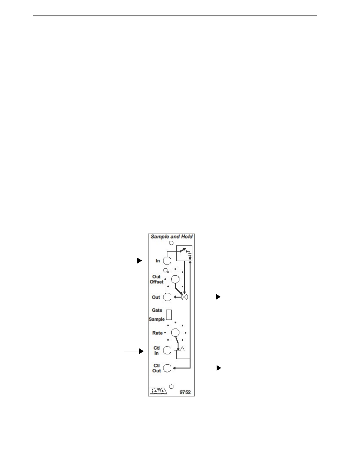
POWERING AND TESTING
Power to the circuit is via a four-circuit, dual-polarity DC power supply. A power connector cable matches the
header for connection with one of the PAiA 977x supplies at 15v or more. Connect the circuit labeled (+) to the
positive DC source (V+), the circuit labeled (-) to the negative DC source (V-), the circuit labeled (G) to the power
ground (G), and the circuit labeled (SG) to the signal ground (SG). For other supplies without separate signal
and power grounds, use two wires to join the two grounds (G and SG) to the one ground (aka GND, 0VDC or
common) at the supply.
Before applying power, check again, to be sure the wiring for the two DC polarities and that the polarized 4ckt
connectors are as intended (see Fig.1B).
Use two-circuit, Tip-Sleeve (TS or mono), cords for patching in or out of the Sample and Hold when connecting
with external devices. Within a 9700-series system, either single conductor (Tip-only), or TS cords may be used.
If this seems confusing, remember that a regular mono cable will always work for most home studios. PAiA
equipment allows tip-only connections for professional applications where star grounding is required.
Test operation by inputting a 0-10V Noise Source such as the 9751 or some other periodic signal such as an
LFO or VCO to the Sample Input and patching the Output from this section to a VCO CV input so the control to
the VCO can be heard. There should be a change controllable with the s/h Rate control, Output Offset control
and Gate/Sample switch settings. Note that as the Offset is adjusted for a more positive CV output range, the
glow will vary more brightly. Offset adjustment helps match the output range attained for a range of input signal
sources which don't necessarily have to be a full 10V range (or DC, ie 0 to +10). Patching the Ctl Out, a copy of
the sampling over to another devices trigger or clock input should elicit an action synchronized to the s/h Output.
An external trigger or clock can be substituted for the internal one by making a patch into the Ctl In.
No is e S o u r ce, VCO, L F O o r oth er
varying, p erio dic v olt ag e.
Select an in sta n taneous, S ample, or
a f ram ed, G ate, co p y o f th e inp u t
volta g e appea ring as CV ou tpu t.
Extern al t rig g er or clock as
sub s titu t e for th e in ternal rat e
co n t rol (d irect clo ck or p o sitive
triggering).
CV o u t p u t , p ro p ort ion al t o the
sampled or g at ed in p u t s ignal
volta g e. A random CV w ith n o is e as
th e input.
Ou tp ut o f th e s am p le rate Clo ck, o r,
a p as s - throug h o f th e exte rnally
ap plied ev ents.
6
Page 7

Notes
DNI marking is Do Not Install note to manufacturer. These are designations where optional capacitors may be
installed, parallel-connecting with capacitors associated with time constants: Cs1/12, 4/13 and 5/15.
Resistor R16 may be installed to parallel or replace on-board resistor R13 to match the current flow for a
substitute LED (subtract the LED voltage from 10v and divide this result by the current (ie 0.01) for the
resistance value).
Mounting holes are provided on the board for custom applications.
7
Page 8

DESIGN ANALYSIS
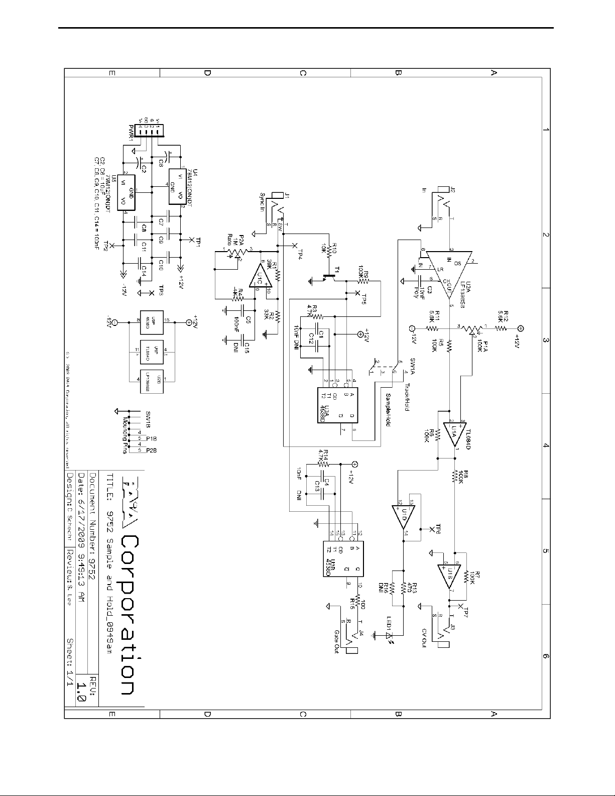
The heart of the sample and hold module is based around the LF398 IC. Samples are taken from an input
on Pin 3 when the (not)SH pin is pulled low and are stored in capacitor C3. When the (not)SH pin is pulled
high, the sample is output from Pin 5 into U1A and U1B which provide output offset scaling as well as
driving the S&H LED through U1D.
The (not)S&H pin is connected to switch SW1, which selects between sample-and-hold and track-and-hold
operation. S&H operation is driven from the U1C square wave oscillator, transistor switch T1 and
monostable multivibrator. The oscillator output is normally connected to the T1 switch through the closed
circuit jack, J1. The transistor circuit then drives the monostable multivibrator which limits the pulse width of
the trigger signal to about 47uS. If an external signal is plugged into J1, the oscillator is taken out of the
circuit. T1 switches at about 1.5V minimum, so just about any signal can be used to control the sample
and hold. When in trigger-and-hold mode, T1 and the 4538 are bypassed and the S&H IC is connected
directly to the J1 input signal. The second 4538 provides a pulse train output in sync with the transistor
switching.
8
Page 9
9752 Parts List
Quan Description Ref Des Marking
( ) 1 9752 PCB Sub-assembly, Sample and Hold
( ) 1 9752 Front Panel, Sample and Hold
( ) 1 100K ohm Potentiometer, 9 mm Snap-In, Linear P1 B100K
( ) 1 1M ohm Potentiometer, 9 mm Snap-In, Audio P2 A1M
( ) 3 Phone Jack, Stereo, 3.5mm J2, J3, J4
( ) 1 Phone Jack, Stereo, 3.5mm, w/switch J1
( ) 1 Switch, Slide, DPDT, RA, PCB Mount SW1
( ) 2 Knob, Set Screw
( ) 1 Shim, Knob, Polyethylene Sleeve
( ) 1 .01uF, 63V Capacitor, Metalized Polyester Film, Radial C3 10nJ63
( ) 1 LED, Yellow Diffused, Through-hole LED1
( ) 1 Header, Vertical, 1row, 4pin PWR1
( ) 1 Cable Assembly, Power, 4-wire
( ) 2 Screw, Self tap, #4 x 3/8, Pan Head Phillips, Black Oxide
Please check the parts against this list. As you locate a part type and verify the quantity (and mounting
hardware -- if required) check it off in the space provided.
Because we have introduced surface-mount parts with these kits, we are providing the printed circuit card as a
sub-assembly with the surface-mount parts already in place.
Also, we want to make you aware that we are using both linear- and audio-taper potentiometers in some of the
modules. They are marked differently so we are asking that you check carefully.
If anything is missing please notify PAiA at [email protected] or by phone at (405) 340-6300, fax (405)
340-6378.
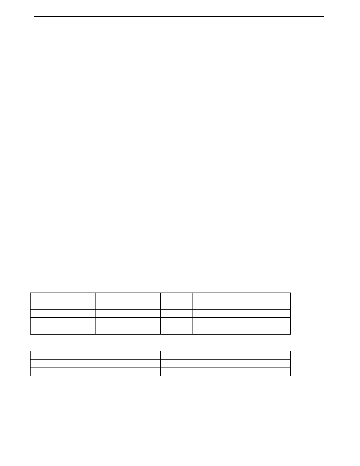
9752 Test Point Data
TP1 +12 VDC TP5 Complement of Internal
Clock
TP2 -12 VDC TP6 LED Voltage
TP3 0 VDC TP7 CV Output
TP4 Internal Clock
9752 Power Requirements Voltage Current
+12 VDC 21.0 mA
-12VDC 33.0 mA
9752 Sample and Hold
9
Page 10
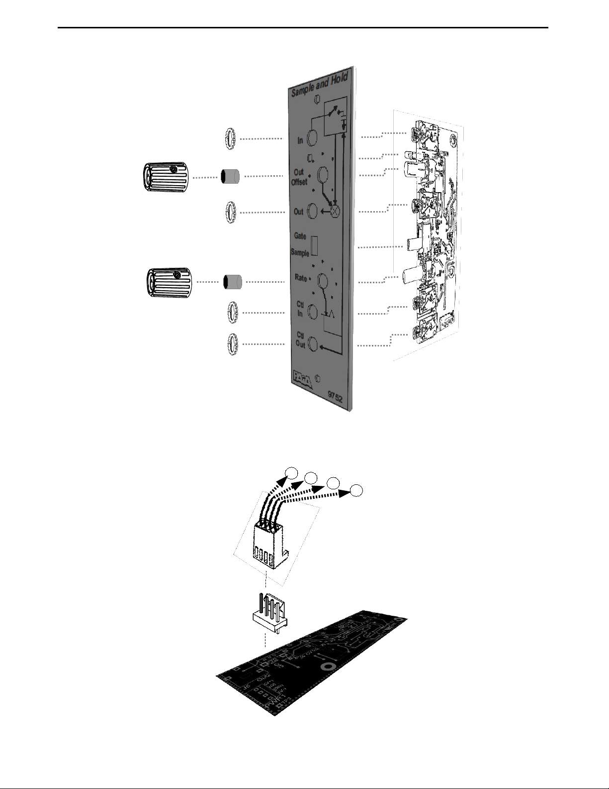
Fig. 1A Attach board to panel using connector nuts, shim control shafts,
and rotate controls to minimum and tighten set-screw knobs to agree.
+
G
SG
-
10
Fig. 1B Orientation of power connector with respect to the printed-circuit-board.
Page 11
E
C
x
o
t
n
e
t
r
r
n
o
a
l
l
I
n
c
p
l
o
u
c
t
k
/
t
r
i
g
g
e
r
1
0
0
K
2
2
0
n
F
G
a
t
e
/
H
o
l
d
C
5
)
.
7
t
C
4
f
o
r
a
n
e
f
f
e
c
t
i
v
e
3
3
0
n
F
(
I
I
t
o
1
0
0
n
F
o
o
5
t
u
e
2
n
:
m
t
e
T
a
d
h
n
i
R
s
u
4
a
s
l
c
t
w
o
h
i
e
1
t
h
m
0
0
c
a
K
h
t
i
a
c
a
n
n
u
g
d
p
e
d
s
a
a
n
o
t
e
f
a
s
s
d
u
d
F
r
e
i
f
g
a
d
.
c
2
2
e
2
o
-
0
f
n
t
h
F
e
N
9
m
a
11
I
C
n
o
t
/
n
E
t
x
r
t
o
c
l
O
l
o
u
c
t
k
p
/
t
u
r
t
i
g
g
e
r
Page 12

12
www.paia.com
 Loading...