

Specification for Approval
PRODUCT NAME:
PRODUCT NO.: PMO8401
CUSTOMER
APPROVED BY
DATE:
PA CER PLC APPROVED
Copyright © 2006 Pacer PLC
- 1 - REV.: A03 2005/04/21
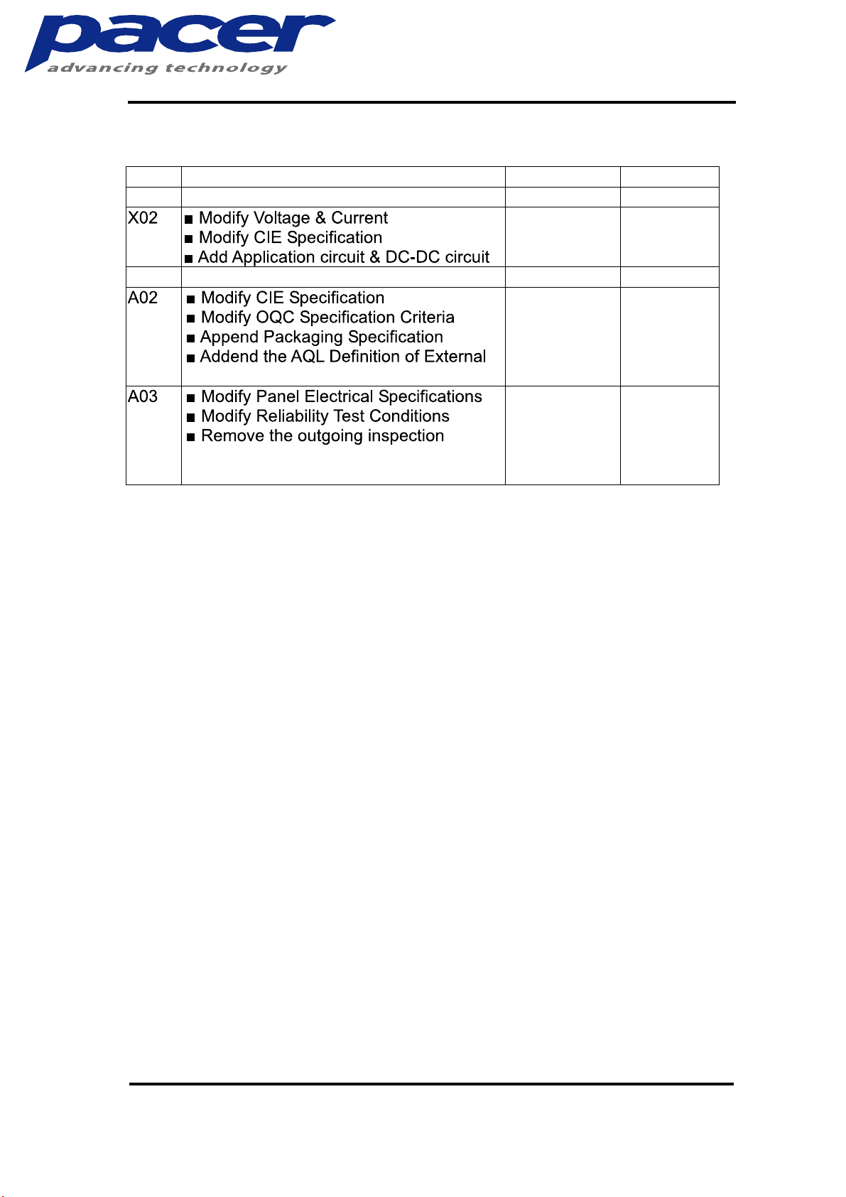
REVISION RECORD
REV. REVISION DESCRIPTION REV. DATE REMARK
X01 INITIAL RELEASE 2003. 09. 04
2003. 11. 28 Page 5, 6, 8
& 9
A01 FORMAL RELEASE 2004. 02. 24
2004. 05. 10 Page 7,19,
20,21,22
Appearance Defect
2005. 04. 21 Page 7, 15
& 21
provision (Refer to “OQC SPEC –
STD – Mono, Area”)
Copyright © 2006 Pacer PLC
- 2 - REV.: A03 2005/04/21
CONTENTS
ITEM PAGE
1. SCOPE
2. FEATURES
3. MECHANICAL DATA
4. MAXIMUM RATINGS
5. ELECTRICAL CHARACTERISTICS
5.1 D.C ELECTRICAL CHARACTERISTICS
5.2 ELECTRO-OPTICAL CHARACTERISTICS
6. INTERFACE
6.1 FUNCTION BLOCK DIAGRAM
6.2 PANEL LAYOUT DIAGRAM
6.3 PIN ASSIGNMENTS
6.4 GRAPHIC DISPLAY DATA RAM ADDRESS MAP
6.5 INTERFACE TIMING CHART
7. POWER ON / OFF SEQUENCE & APPLICATION CIRCUIT
7.1 POWER ON / OFF SEQUENCE
7.2 APPLICATION CIRCUIT
7.3 COMMAND TABLE
8. RELIABILITY TEST CONDITIONS
9. EXTERNAL DIMENSION
10. PACKING SPEC IFIC ATION
1 1. APPENDIXES
4
4
5
5
6
8
12
15
16
22
23
Copyright © 2006 Pacer PLC
- 3 - REV.: A03 2005/04/21

1. SCOPE
This specification is to define the general provisions and quality requirements
that apply to the supply of display cells manufactured by Pacer. This
document, together with the Module Ass’y Drawing, is the highest-level
specification for this product.
2. FEATURES
- Two Area color small molecular organic light emission diode
- Color: Blue/Yellow
- Panel matrix: 128*64
- Driver IC: SSD1303
- Excellent quick response time.
- Extremely thin thickness for best mechanism design: 2.05mm
- High contrast. 100:1
- Wide viewing angle. 160
- 8-bit 6800-series parallel interface, 8-bit 8080-series parallel interface,
serial peripheral
- Wide range of operating temperature : -20 to 70 °C
Copyright © 2006 Pacer PLC
- 4 - REV.: A03 2005/04/21
3. MECHANICAL DATA
NO ITEM SPECIFICATION UNIT
1 Dot Matrix 128 (W) x 64 (H) dot
2 Dot Size 0.18 (W) x 0.21 (H) mm
3 Dot Pitch 0.20 (W) x 0.23 (H) mm
4 Aperture Rate 82 %
5 Active Area 25.58 (W) x 15.18 (H) mm
6 Panel Size 33.0 (W) x 23.0 (H) mm
2
2
2
2
7 Panel Thickness
2.05 0.1
8 Module Size 33.0 (W) x 37.5 (H) x 2.05 (T) mm
mm
3
9 Diagonal A/A size 1.2 inch
10 Module Weight
3.0 10%
gram
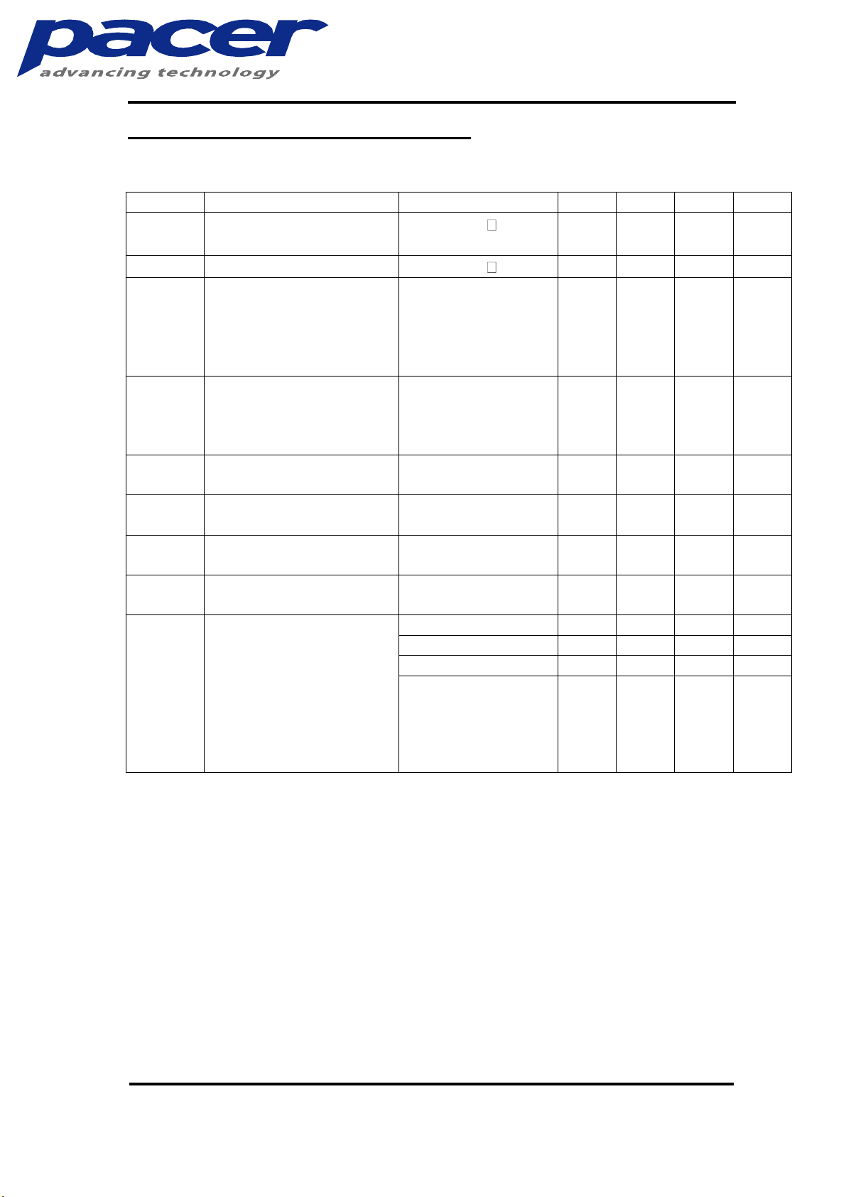
4. MAXIMUM RATINGS
ITEM MIN MAX UNIT Condition
Supply Voltage (VDD) -0.3 3.5 V Ta = 25°C
Supply Voltage(Vcc) 8 16 V Ta = 25°C
Operating Temp. -20 70 °C
Storage Temp -40 85 °C
Humidity - 85 %
30cd/m2, 20% pixels
Operating Life Time 8,000 - Hrs
scrolling
display on at 85Hz frame
Storage Life Time 20,000 - Hrs Ta=25°C, 50% RH
Note:
(A) Under Vcc = 12 Volts, Ta = 25°C, 50% RH.
(B) Operating Life Time is defined when the luminance has decayed to less than
(C) The storage life time is define as 25% di mension shrinking of initial value
Copyright © 2006 Pacer PLC
50% of the initial measured luminance before life test.
and luminance
minimum luminance under temperature
25°C, RH<50%,
- 5 - REV.: A03 2005/04/21
5. ELECTRICAL CHARACTERISTICS
5.1 D.C ELECTRICAL CHARACTERISTICS
SYMBOL PARAMETERS
V
V
CC
DD
Analog power supply
(for OLED panel)
Digital power supply
Operating current for V
VDD = 2.7V, VCC = 12V,
I
DD
IREF = 10uA
No loading, All Display
ON
Operating current for V
I
CC
VDD = 2.7V, VCC = 12V,
IREF = 10uA
All Display ON
VIH Hi logic input level
VIL Low logic input level
VOH Hi logic output level
VOL Low logic output level
Segment on output
current
VDD=2.7V, VCC=12V,
I
SEG
IREF=10uA, Display on,
Segment
pin under test is
connected with a
20K resistive load to V
TEST CONDITION MIN TYP MAX UNIT
Ta=-20 C to
Ta=-20
DD
Contrast=FF - 190 - uA
CC
Contrast=FF - 550 - uA
Contrast=FF - - 300 uA
Contrast=AF - 220 - uA
Contrast=5F - 120 - uA
Contrast=0F
SS
11.5 12 12.5
C to
0.8*
0.9*
2.4 2.7 3.5
VDD
- VDD
0 -
VDD
- VDD
0 -
- 20 -
0.2*
VDD
0.1*
VDD
V
V
V
V
V
V
uA
Copyright © 2006 Pacer PLC
- 6 - REV.: A03 2005/04/21
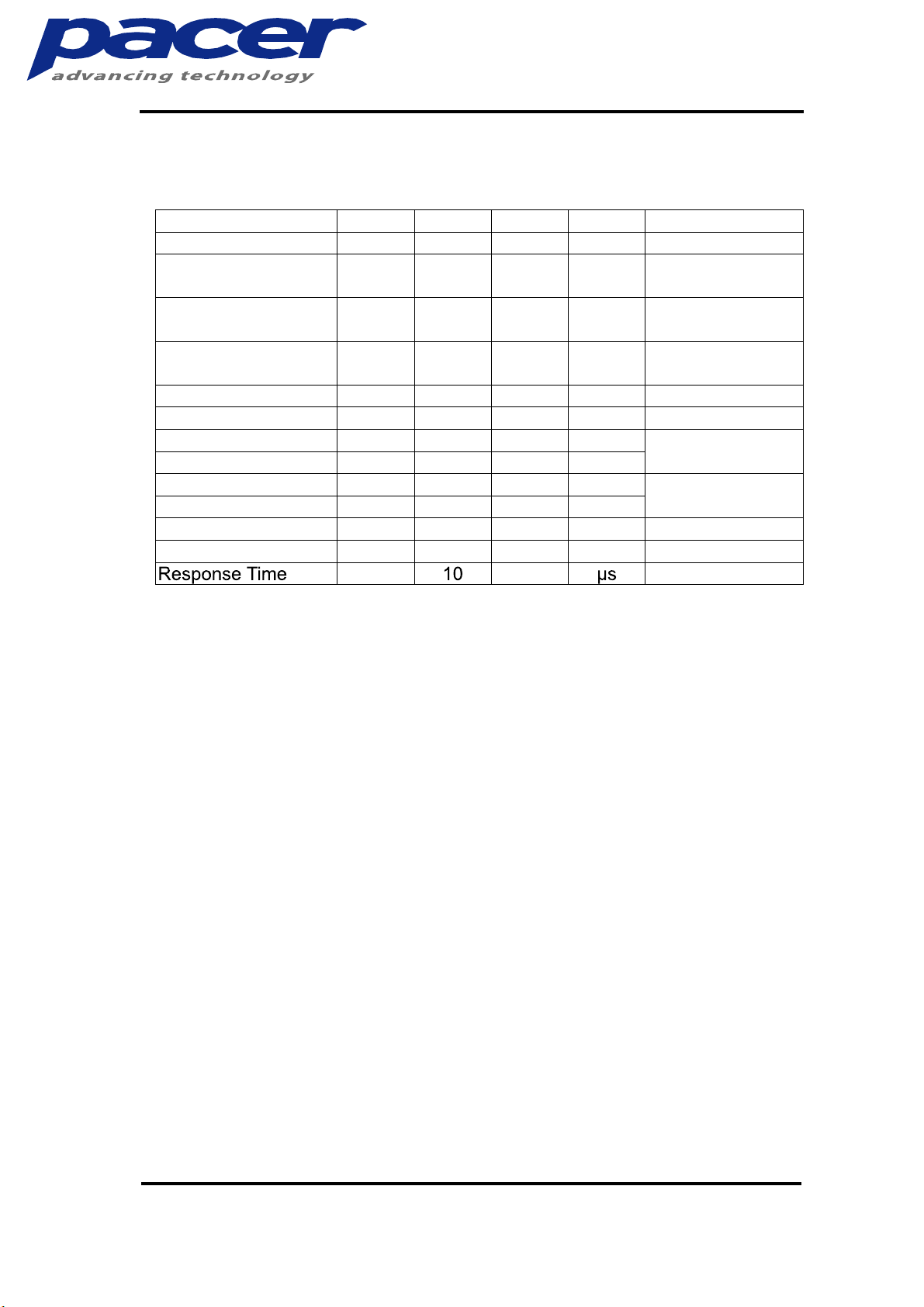
5.2 ELECTRO-OPTICAL CHARACTERISTI CS
r
PANEL ELECTRICAL SPECIFICATIONS
PARAMETER MIN TYP. MAX UNITS COMMENTS
Normal mode current - 7 9 mA All pixels on (1)
Standby mode
current
Normal mode power
consumption
Standby mode powe
consumption
1 2 mA
- 84 108 mW All pixels on (1)
12 24 mW
Standby mode
10% pixels on (2)
Standby mode
10% pixels on (2)
Normal Luminance 40 45 cd/m2 Display Average
Standby Luminance 10 cd/m2 Display Average
CIEx(Blue) 0.12 0.15 0.18
CIEy(Blue) 0.22 0.27 0.32
CIEx(Yellow) 0.42 0.46 0.50
CIEy(Yellow) 0.46 0.50 0.54
x, y (CIE 1931)
x, y (CIE 1931)
Dark Room Contrast 100:1
Viewing Angle 160 degree
(1) Normal mode condition :
- Driving Voltage : 12V
- Contrast setting : 0x4F
- Frame rate : 85Hz
- Duty setting : 1/64
(2) Standby mode condition :
- Driving Voltage : 12V
- Contrast setting : 0x0C
- Frame rate : 85Hz
- Duty setting : 1/64
Copyright © 2006 Pacer PLC
- 7 - REV.: A03 2005/04/21

6. INTERFACE
6.1 FUNCTION BLOCK DIAGRAM
SSD1303 TAB
NC
Vss
VDD
Inte r fac e select io n
CS#
RES#
D/C
WR#
RD#
DATA BUS
IREF
VCOMH
VCC
SSD1303
Row 1 -63
Column 0-127
Row 0 -62
128x64
OLED Panel
Pacer 128X64 OLED Module
6.2 PANEL LAYOUT DIAGRAM
- 8 - REV.: A03 2005/04/21
Copyright © 2006 Pacer PLC

6.3 PIN ASSIGNMENTS
A
A
PIN NAME PIN NO. TYPE DESCRIPTION
NC 1 - No connection
VSS 2 I This is a ground pin.
Test 0 3 - Reserved pin; No connection and left float
Test 1 4 - Reserved pin; No connection and left float
Test 2 5 - Reserved pin; No connection and left float
Test 3 6 - Reserved pin; No connection and left float
Test 4 7 - Reserved pin; No connection and left float
NC 8 - No connection
NC 9 - No connection
NC 10 - No connection
VDD 11 I Voltage power supply for logic
BS1 12 I MCU interface selection input
BS2 13 I MCU interface selection input
NC 14 - No connection
CS# 15 I This is a chip select control pin.
RES# 16 I Hardware reset signal
D/C# 17 I This is a Data/Command control pin.
WR# 18 I This pin is used to receive the Write Data signal.
RD# 19 I This pin is used to receive the Read Data signal.
D0 20 I/O This pin is bi-direction data signal
D1 21 I/O This pin is bi-direction data signal
D2 22 I/O This pin is bi-direction data signal
D3 23 I/O This pin is bi-direction data signal
D4 24 I/O This pin is bi-direction data signal
D5 25 I/O This pin is bi-direction data signal
D6 26 I/O This pin is bi-direction data signal
D7 27 I/O This pin is bi-direction data signal
I
28 I
REF
V
29 I
COMH
resistor should be connected between this pin
and V
SS
capacitor should be connect between this pin
and VSS
VCC 30 I Positive high voltage power supply
NC 31 - No connection
Copyright © 2006 Pacer PLC
- 9 - REV.: A03 2005/04/21

6.4 GRAPHIC DISPLAY DATA RAM ADDRESS MAP
Copyright © 2006 Pacer PLC
- 10 - REV.: A03

6.5 INTERFACE TIMING CHART
Copyright © 2006 Pacer PLC
- 11 - REV.: A03

7. POWER ON / OFF SEQUENCE & APPLICATION CIRCUIT
7.1 POWER ON / OFF SEQUENCE
Display turn on
DC-DC power off
(VCC turn off)
VDD power on
Hardware RESET
RESET time depends
on driver IC datasheet
Display off
Driver IC initial
sequence
DC-DC power on
(VCC turn on)
Wait 100m s for
VCC stable
Display on
Display start and
end address setting
Send display data
Display turn off
sequence
Send display off
command
DC-DC power off
(VCC turn off)
Wait 100ms for
VCC reach 0V
VDD power turn off
To protect OLED panel and extend the panel lifetime, the driver IC pow er up/down
routine should include a delay period between high voltage and low voltage power
sources turn on/off.
Power up Sequence:
1. Power up Vdd
2. Hardware RESET
3. Send display off command
4. Power up Vcc
5. Delay 100ms (when Vcc is stable)
6. Send Display on command
On Vdd On Vcc Display On Display Off Off Vcc Off Vdd
VCC
VDD
GND
Power down Sequence:
1. Send Display off command
2. Power down Vcc
3. Delay 100ms (When Vcc is reach 0
and panel is completely discharges)
4. Power down Vdd
VCC
VDD
GND
Copyright © 2006 Pacer PLC
- 12 - REV.: A03

7.2 APPLICA TION CIRCUIT
Copyright © 2006 Pacer PLC
- 13 - REV.: A03

DC-DC Circuit
7.3 COMMAND TABLE
Refer to SSD1303 IC Spec.
Copyright © 2006 Pacer PLC
- 14 - REV.: A03

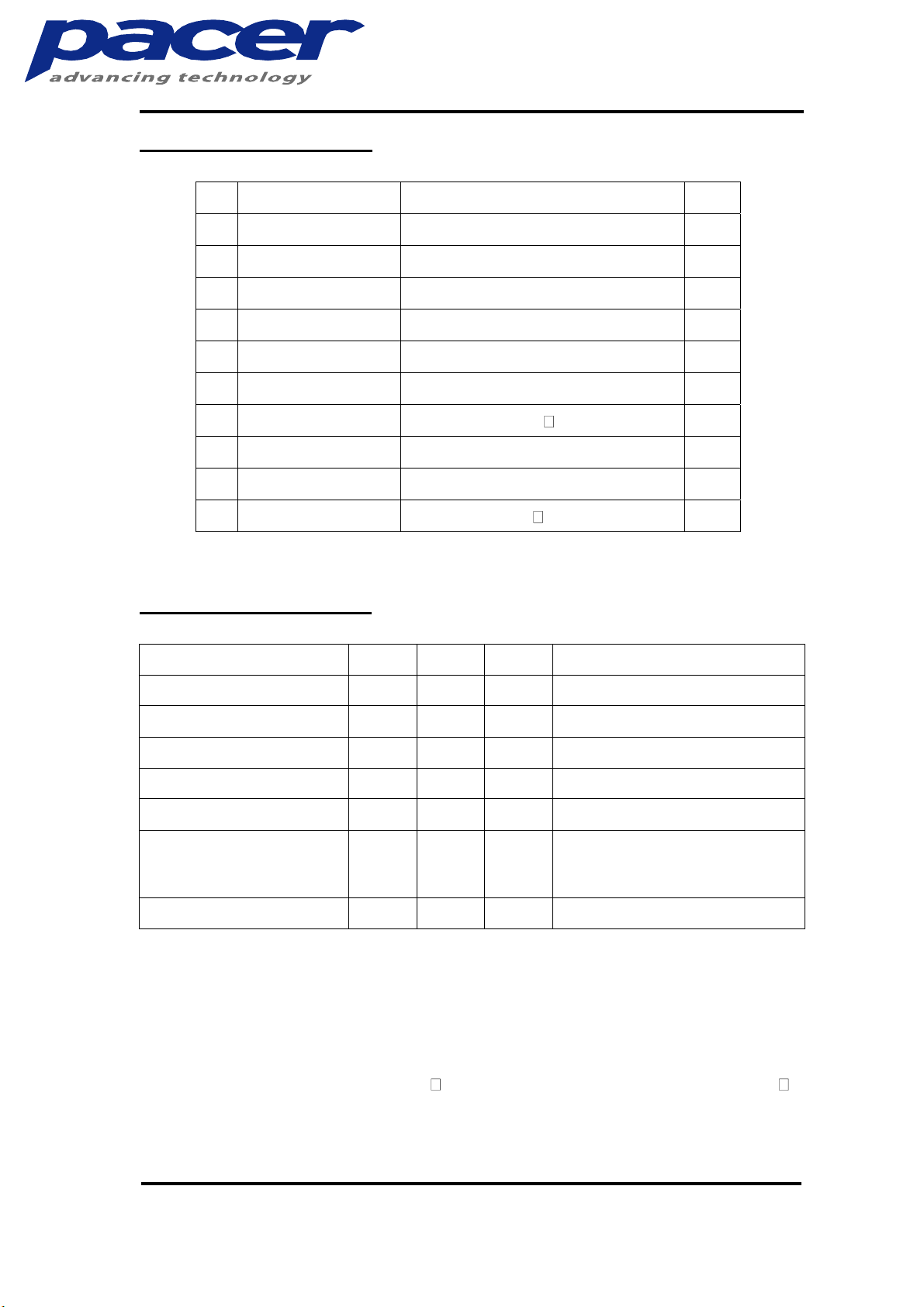
8. RELIABILITY TEST CONDITIONS
No. Items Specification Quantity
High temp.
1
(Non-operation)
Low temp.
2
(Non-operation)
3 High te mp. (Operation) 70°C, 120hrs 3
4 Low temp. (Operation) -20°C, 120hrs 2
High temp. / High
5
humidity (Non-operation)
High temp. / High
6
humidity (Operation)
85°C, 240hrs 3
-40°C, 240hrs 2
85°C, 85%RH, 120hrs 5
65°C, 90%RH, 120hrs 5
Thermal shock
7
(Non-operation)
OLB Peel strength
8
(Non-operation)
9 Vibration
10 Drop
11 ESD (Non-operation)
Test and measurement conditions
1. All measurements shall not be started until the specimens attain to
temperature stability.
-40°C ~85°C (-40°C /30min;
transit /3min; 85°C /30min; transit
/3min) 1cycle: 66min, 100 cycles
500g/cm(Speed~ 50mm/min) 5
Frequency : 5~50HZ, 0.5G
Scan rate : 1 oct/min
Time : 2 hrs/axis
Test axis : X, Y, Z
Height: 120cm
Sequence : 1 angle 3 edges and
6 faces
Cycles: 1
Air discharge model, ±8kV, 10
times
2
1 Carton
1 Carton
5
2. All-pixels-on is used as operation test pattern.
3. The degradation of Polarizer are ignored for item 1, 5 & 6.
Evaluation criteria
1. The function test is OK.
2. No observable defects.
3. Luminance: > 50% of initial value.
4. Current consumption: within ± 50% of initial value.
Copyright © 2006 Pacer PLC
- 15 - REV.: A03

9. EXTERNAL DIMENSION
NC
TEST 0
SYMBOLNO.
VSS
1
3
2
Pin Assignment
New Design
Modify Polarizer Tolerance
Add Seal Dim. & Modify Glass Tolerance
TEST 1
TEST 2
456
TEST 4
TEST 3
0.2
NC
0.18
NC
987
NC
VDD
10
11
NC
BS2
CS#
12 BS1
131416
15
0.02
R/W#
RES#
17 D/C#20191821
D0D1D2
E(/RD)
03
D5D6D7
D3
D4
22
2627252324
0.5
VCC
VCOMH
28 IREF3031
29
NC
1
0
4
8
O
M
P
03
9608401000
Module Ass'y
08/27/2003
1/1
128x56 Blue
Eric Wu
mm
Ju Guan Chen
1:0.55
David Li
Paul Chang
Arthur Chen
seal
0.7Max.
03
16.5±0.2
2.5
0.21
0.23
(Seal)
1.15Max.
03
2
1.8
(Seal)
4.0
0.02
1.0 max
0.7
25.58
128x8 Yellow
1.82 12.86
A
Specification
Pin 1
128x64
OLED(Y/B)
2.Dot Matrix:
1.Display:
0.20x0.23mm
0.18x0.21mm
4.Dot Pitch:
3.Dot Size:
82%
5.Apertuer Rate:
25.58x15.18mm
SSD1303T6
6.Active Area:
7.IC:
12/04/2003
06/03/2004
01
02
03
C62 C0 S0 S127 C1 C63
2.05±0.1
0.2(Polarizer)
0.7
2.5 Max.
03
1.5 Max.
03
(Seal)
(Seal)
20.5±0.25(Cover)
03
03
W=0.4±0.02
33.0±0.25
31.0±0.3(Polarizer) (1)
(2.51) 15.18(A/A)
Copyright © 2006 Pacer PLC
25.58(A/A) (3.71)
18.5±0.3(Polarizer)(1)
128x64 Dots
23.0±0.25
03
37.5
(2)
27.83±0.2
26.64±0.2 (Slit)
22.0±0.1(Alignment hole)
P0.845x(31-1)=25.35±0.025
)
R
S
(
7
.
0
I
R
-
P
2
(
5
.
0
R
-
2
4.0
)
e
l
o
h
- 16 - REV.: A03

10. PACKING S PECIF IC ATION
x 12 pcs
x2 pcs
ONY/LDPE,285x90x480mm
Packing Instruction
3003000012
5
03/05/2004
01
x 1 pcs(empty)
3001000003
Pizza Box 345x285x88mm,B
6
x 10 pcs
x 1 pcs(empty)
4G ( )
3000000500
4
3000000007
7
Carton 385x305x203mm,AB
x10
PM08401
Packing Instruction
1/1
mm
Eric Wu
01
1:9
Ju Guan Chen
Eric Wu
2
2
10
20
24
480
QTY
1
Paul Chang
x 10 pcs
EPE COVER FOAM 290x232x2mm For P084
3002000029
3
Arthur Chen
DESC
3008000014
Tray 330x270x11.7mm,T=0.7mm,PS,P084
2
TAB PANEL ASS'Y FOR PF08401
Tray 330x270x11.7mm,T=0.7mm,PS,P084
EPE COVER FOAM 286.6x229.6x2mm For P084
ONY/LDPE,285x90x480mm
4G ( )
Carton 385x305x203mm,AB
Pizza Box 345x285x88mm,B
Bottom up
PART No.
x 24 pcs
9608401000
TAB Panel Ass'y For P08401
1
ITEM
9608401000
1
3008000014
2
3002000029
3
3000000500
3003000012
476
5
3001000003
3000000007
- 17 - REV.: A03
Copyright © 2006 Pacer PLC

1 1. APPENDIXES
APPENDIX 1: DEFINITIONS
A. DEFINITION OF CHROMATICITY COORDINATE
The chromaticity coordinate is defined as the coordinate value on the CIE
1931 color chart for R, G, B, W.
B. DEFINITION OF CONTRAST RATIO
The contrast ratio is defined as the following formula:
Luminance of all pixels on measurement
Contrast Ratio =
Luminance of all pixels off measurement
C. DEFINITION OF RESPONSE TIME
The definition of response time (Tr, Tf) is the time interval from turn on state
to turn off state or vice versa, which is shown in Figure 2.
100%
90%
Brightness
T r
T f
Figure 2: Response time
10%
Copyright © 2006 Pacer PLC
- 18 - REV.: A03

D. DEFINITION OF VIEWING ANGLE
The viewing angle is defined as Figure 3.
-
direction)
(
+ y
= 0
+
-
+
-
+
- x
x
direction)
(
+ y
-
= 0
+
-
Figure 3: Viewing Angle
Copyright © 2006 Pacer PLC
- 19 - REV.: A03

APPENDIX 2: MEASUREMENT APPARATUS
A. LUMINANCE/COLOR COORDINATE
PHOTO RESEARCH PR-705, MINOLTA CS-100
Measurement
Header
Panel
Plate Form
B. CONTRAST / RESPONSE TIME / VIEW ANGLE
WESTAR CORPORATION FPM-510
Measurement
Header
PR-705 /
MINOLTA CS-100
Color Analyzer
Westar FPM-510
Plate Form
Copyright © 2006 Pacer PLC
Panel
Display Contrast /
Response time /
View angle Analyzer
- 20 - REV.: A03

C. PEEL STRENGTH
e
e
Force
Gauge
DPZ-50N
Fixtur
Film
Panel
Fixtur
D. ESD ON AIR DISCHARGE MODE
R 330 ohms
DISCHARGE
TIP
V
C
150pF
RETURN
ESD
EUT
GROUND PLANE
Copyright © 2006 Pacer PLC
- 21 - REV.: A03

APPENDIX 3: PRECAUTIONS
A. RESIDUE IMAGE
Because the pixels are lighted in different time, the luminance of active pixels
may reduce or differ from inactive pixels. Therefore, the residue image will
occur. To avoid the residue image, every pixel needs to be lighted up
uniformly.
Copyright © 2006 Pacer PLC
- 22 - REV.: A03
 Loading...