


Preliminary Specification
PRODUCT NAME : 1.3” 128X96 White OLED
PRODUCT NO.: PMO14201
APPROVED BY
DATE:
PACER PLC. APPROVED
Copyright © 2006 Pacer PLC
- 1 - REV.:X02 2006/03/01

REVISION RECORD
REV. REVISION DESCRIPTION REV. DATE REMARK
X01 INITIAL RELEASE 2006. 01. 12
X02 Add the operating conditions for
different luminance
Add the panel electrical specification
Modify the CIE specification
Add the application circuit
2006. 03. 01 Page 6, 7, 8 &
17
.
Copyright © 2006 Pacer PLC
- 2 - REV.:X02 2006/03/01
CONTENTS
ITEM PAGE
1. SCOPE
2. WARRANTY 4
3. FEATURES 4
4. MECHANICAL DATA
5. MAXIMUM RATINGS 6
6. ELECTRICAL CHARACTERISTICS 7
6.1 D.C ELECTRICAL CHARACTERISTICS
6.2 ELECTRO-OPTICAL CHARACTERISTICS
7. INTERFACE 10
7.1 FUNCTION BLOCK DIAGRAM
7.2 PANEL LAYOUT DIAGRAM
7.3 PIN ASSIGNMENTS
7.4 GRAPHIC DISPLAY DATA RAM ADDRESS MAP
7.5 INTERFACE TIMING CHART
8. POWER ON / OFF SEQUENCE & APPLIC ATION CIRCUIT
8.1 POWER ON / OFF SEQUENCE
8.2 APPLICATION CIRCU IT
8.3 COMMAND TABLE
9. RELIABILITY TEST CONDITIONS 18
10. EXTERNAL DIMENSION
11. PACKING SPECIFICATION 20
12. APPENDIXES 21
4
5
16
19
Copyright © 2006 Pacer PLC
- 3 - REV.:X02 2006/03/01
1. SCOPE
The purpose of this specification is to define the general provisions and quality
requirements that apply to the supply of display cells manufactured by
RiTdisplay. This document, together with the Module Ass’y Drawing, is the
highest-level specification for this product. It describes the product, identifies
supporting documents and contains specifications.
2. WARRANTY
Pacer PLC warrants that the products delivered pursuant to this specification (or
order) will conform to the agreed specifications for twelve (12) months from the
shipping date ("Warranty Period").Pacer PLC is obligated to repair or replace
the products which are found to be defective or inconsistent with the
specifications during the Warranty Period without charge, on condition that the
products are stored or used as the conditions specified in the specifications.
Nevertheless, Pacer PLC is not obligated to repair or replace the products
without charge if the defects or inconsistency are caused by the force majeure
or the reckless behaviors of the customer.
After the Warranty Period, all repairs or replacements of the products are
subject to charge.
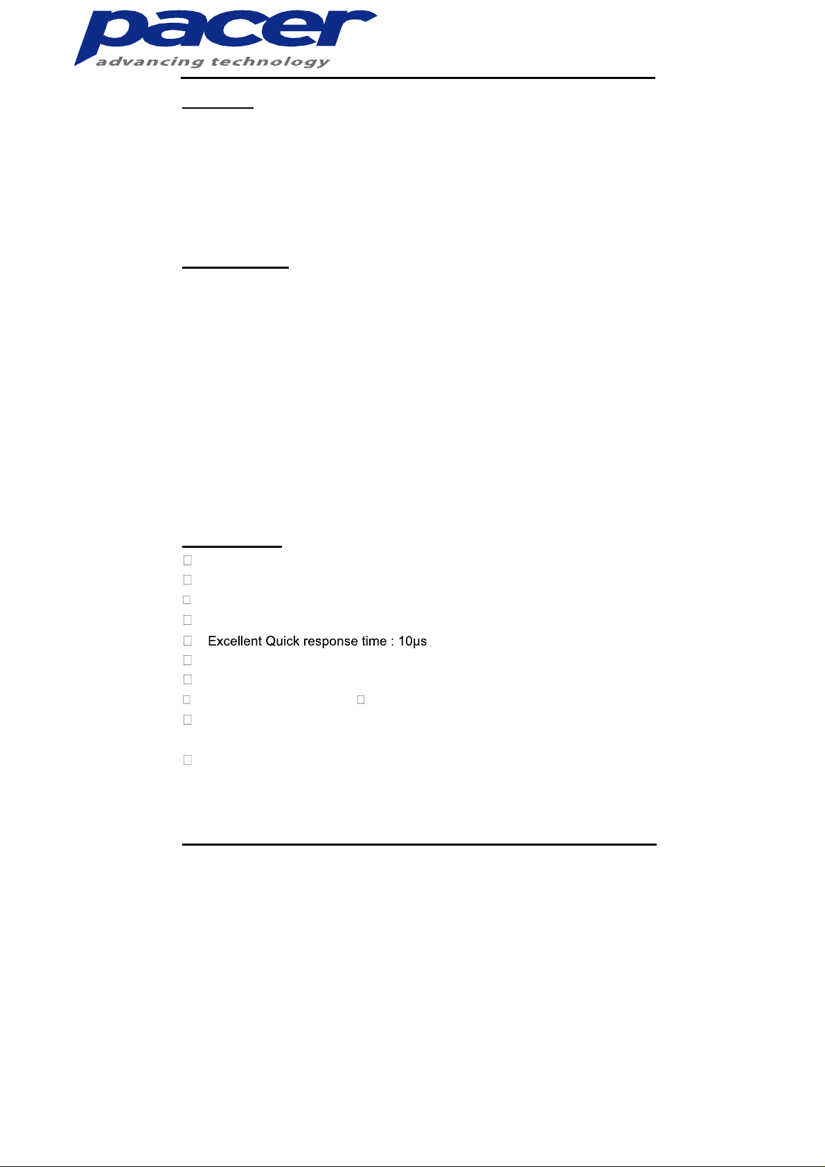
3. FEATURES
Small Molecular Passive Organic Light Emission Diode.
Color : White
Panel matrix : 128*96
Driver IC : SSD1329U2
Extremely thin thickness for best mechanism design : 1.65mm.
High contrast : 500:1
Wide viewing angle : 16 0
8-bit 6800-series Parallel Interface, 8-bit 8080-series Parallel Interface,
Serial Peripheral Interface.
Wide range operating temperature : -40 to 70 °C
- 4 - REV.:X02 2006/03/01
Copyright © 2006 Pacer PLC
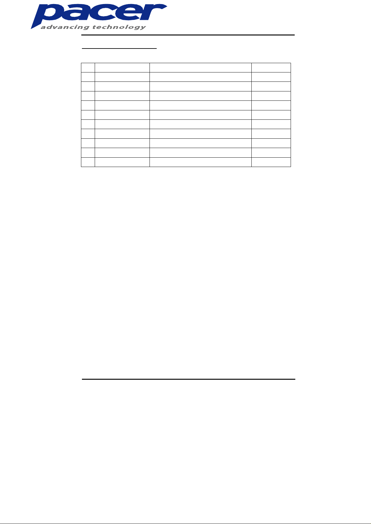
4. MECHANICAL DATA
NO ITEM SPECIFICATION UNIT
1 Dot Matrix 128 (W) x 96 (H) dot
2 Dot Size 0.19 (W) x 0.19 (H) mm
3 Dot Pitch 0.21 (W) x 0. 21 (H) mm
4 Aperture Rate 82 %
5 Active Area 26.86 (W) x 20.14 (H) mm
6 Panel Size 33 (W) x 26.8 (H) mm
7 Panel Thickness 1.65 mm
8 Module Size 33 (W) x 41.6 (H) x 1.65 (T) mm
9 Diagonal A/A size 1.3 inch
10 Module Weight TBD gram
2
2
2
2
3
Copyright © 2006 Pacer PLC
- 5 - REV.:X02 2006/03/01
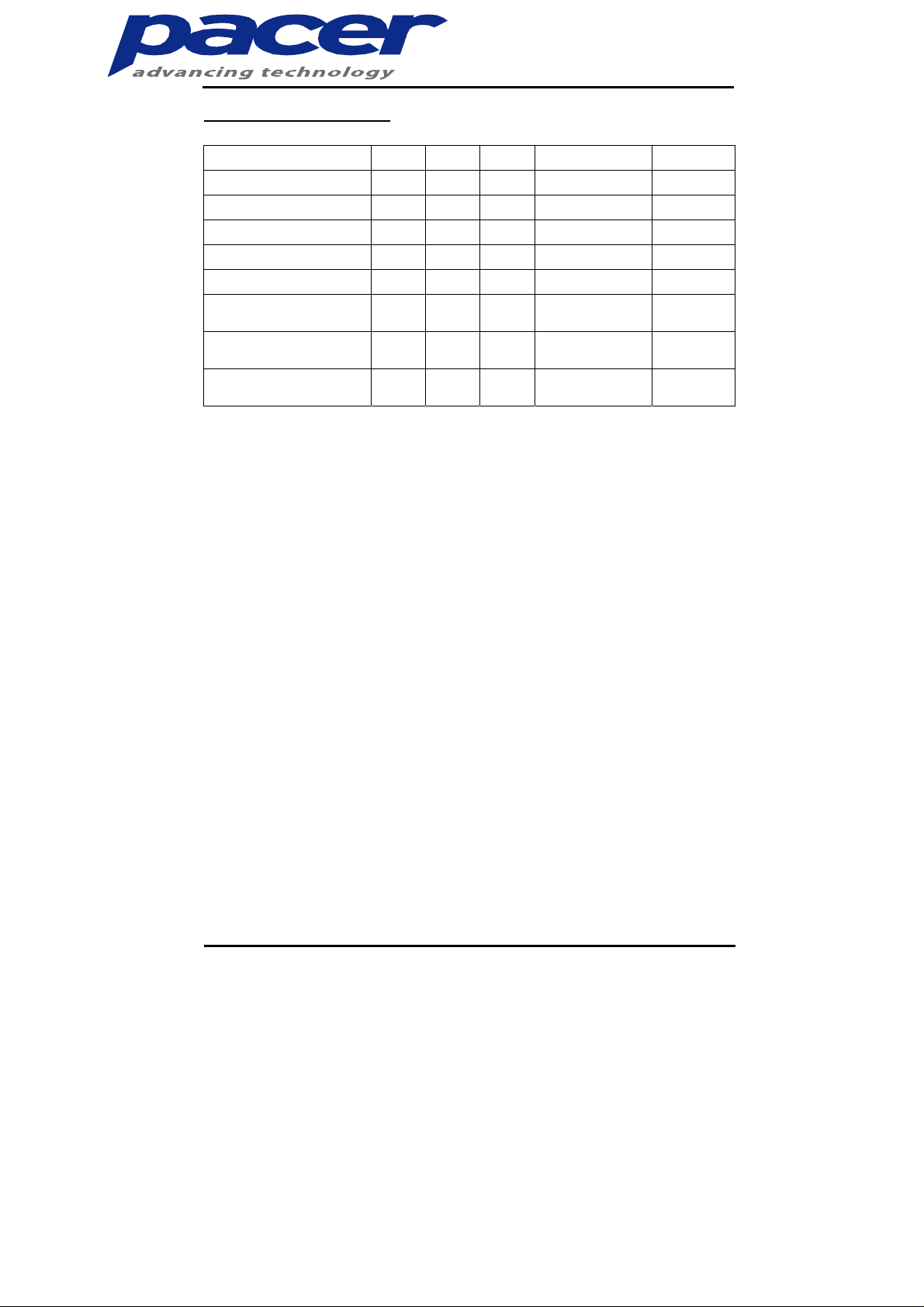
5. MAXIMUM RATINGS
ITEM MIN MAX UNIT Condition Remark
Supply Voltage (VDD) -0.3 3.5 V Ta = 25°C
Supply Voltage(Vcc) 8 16 V Ta = 25°C
Operating Temp. -40 70 °C
Storage Temp -40 85 °C
Humidity 85 %
Operating Life Time 8,000 - Hrs
Operating Life Time 10,000 - Hrs
Operating Life Time 12,500 - Hrs
Note:
(A) Under Vcc = 15V, Ta = 25°C, 50% RH.
(B) Life time is defined the amount of time when the luminance has decayed
to less than 50% of the initial measured luminance.
(1) Setting of 120cd/m² :
- Contrast setting : 0xEC
- Frame rate : 85Hz
- Duty setting : 1/96
(2) Setting of 100cd/m² :
- Contrast setting : 0xB7
- Frame rate : 85Hz
- Duty setting : 1/96
(3) Setting of 80cd/m² :
- Contrast setting : 0x82
- Frame rate : 85Hz
- Duty setting : 1/96
120 cd/m², 50%
checkerboard
100 cd/m², 50%
checkerboard
80 cd/m², 50%
checkerboard
Note (1)
Note (2)
Note (3)
Copyright © 2006 Pacer PLC
- 6 - REV.:X02 2006/03/01

6. ELECTRICAL CHARACTERISTICS
6.1 D.C ELECTRICAL CHARACTERISTICS
SYMBOL PARAMETERS TEST CONDITION MIN TYP MAX UNIT
Driver power supply
V
CC
(for OLED panel)
Logic operating
V
DD
voltage
Ta=-20°C to +70°C 2.4 2.7 3.5 V
VOH Hi logic output level
VOL Low logic output level
VIH Hi logic input level
VIL Low logic output level
Operating current for
I
CC
Operating current for
I
DD
Segment output
I
SEG
Contrast=7F - 750 850 uA
V
CC
Contrast=7F - 72 200 uA
V
DD
current
Ta=-20°C to +70°C 14.5 15 15.5 V
Iout=100 uA,
3.3MHz
Iout=100uA,
3.3MHZ
0 -
Iout=100uA,
3.3MHZ
Iout=100uA,
3.3MHZ
0 -
Contrast=7F
Contrast=5F
Contrast=3F
Contrast=1F
0.9*
- VDD V
V
DD
0.1*
V
DD
0.8*
- VDD V
V
DD
0.2*
V
DD
250 300 370
- 225 -
- 150 50 75 100
V
V
uA
uA
uA
uA
Note : VDD=2.7 V VCC= 15 V Frame rate= 85 Hz No panel attached.
- 7 - REV.:X02 2006/03/01
Copyright © 2006 Pacer PLC
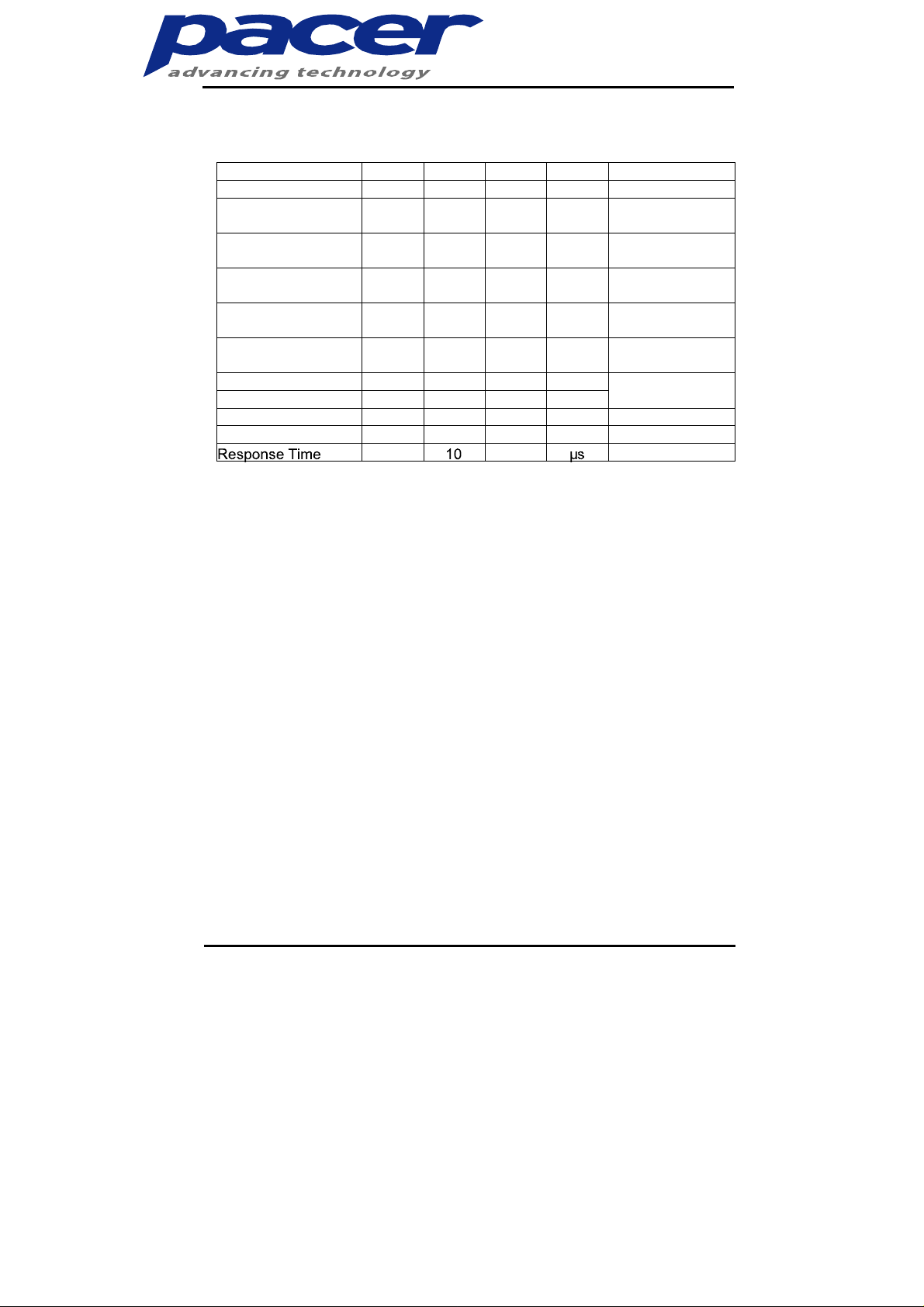
6.2 ELECTRO-OPTICAL CHARAC TERIST ICS
r
P ANEL ELECTRICAL SPEC IFICATIONS
PARAMETER MIN TYP. MAX UNITS COMMENTS
Normal mode current - 24 mA All pixels on (1)
St an dby m o de
current
Normal mode power
consumption
consumption
Normal mode
Luminance
St andby mode
Luminance
1 mA
- 360 mW All pixels on (1)
tandby mode powe
15 mW
80 100 cd/m
10 cd/m
CIEx(White) 0.24 0.28 0.32
CIEy(White) 0.30 0.34 0.38
x, y (CIE 1931)
Standby mode
10% pixels on (2)
Standby mode
10% pixels on (2)
Display Average
2
Display Average
2
Dark Room Contrast 500:1
Viewing Angle 160 degree
(1) Normal mode condition :
- Driving Voltage : 15V
- Contrast setting : 0xB7
- Frame rate : 85Hz
- Duty setting : 1/96
(2) Standby mode condition :
- Driving Voltage : 15V
- Contrast setting : 0x00
- Frame rate : 85Hz
- Duty setting : 1/96
- 8 - REV.:X02 2006/03/01
Copyright © 2006 Pacer PLC

7. INTERFACE
7.1 FUNCTION BLOCK DIAGRAM
TAB
BS1
BS2
E/RD# Column 0~127
R/W#
D/C#
RES#
CS#
Data Bus(D0~D7)
VCC
VDD
VDDIO
VCOM H
VCIR Row 32~127
VSS
LVSS
SSD1329
128X96
OLED Panel
7.2 PANEL LAYOUT DIAGRAM
Copyright © 2006 Pacer PLC
- 9 - REV.:X02 2006/03/01

7.3 PIN ASSIGNMENTS
PIN
PIN NO DESCRIPTION
NAME
NC 1 No connection.
VCIR 2 No connection and left float.
VCOMH 3
Com Voltage Output. Acapacitor should be connected
between this pin and V
LVSS 4 Ground.
VSS 5 Ground.
BS1 6
MCU parallel interface selection input.
BS2 7
SS
.
IREF 8
Reference current input pin.
A resistor should be connected between this pin and VSS.
CS# 9 Chip select input.
RES# 10
Reset signal input.
When it’s low, initialization of SSD1329 is executed.
Data/ Command control.
D/C# 11
Pull high for write/read display data.
Pull low for write command or read status.
R/W# 12
E 13
MCU interface input.
Data write operation is initiated when it’s pull low.MCU
interface input. Data read operation is initiated when it’s
pull low.
D0 14 Data bus(for parallel interface)
D1 15 Data bus(for parallel interface)
D2 16 Data bus(for parallel interface)
D3 17 Data bus(for parallel interface)
D4 18 Data bus(for parallel interface)
D5 19 Data bus(for parallel interface)
D6 20 Data bus(for parallel interface)
D7 21 Data bus(for parallel interface)
VDDIO 22 This pin is a power supply pin of I/O buffer.
VDD 23 Power supply for logic.
VCC 24 Power supply for analog circuit.
NC 25 No connection.
Copyright © 2006 Pacer PLC
- 10 - REV.:X02 2006/03/01

7.4 GRAPHIC DISPLAY DATA RAM ADDRESS MAP
GDDRAM Address Map - Horizontal Address Increment A[2]=0, Column Address Re-map A[0]=0, Nibble Re-map
A[1]=0, COM Re-map A[4]=0, Display Start Line=00H (Data byte sequence: D0, D1, D2 … D8191)
GDDRAM Address Map - Vertical Address Increment A[2]=1, Column Address Re-map A[0]=0, Nibble Re-map
A[1]=0, COM Re-map A[4]=0, Display Start Line=00H (Data byte sequence: D0, D1, D2 … D8191)
GDDRAM Address Map - Horizontal Address Increment A[2]=0, Column Address Re-map A[0]=1, Nibble Re-map
A[1]=1, COM Re-map A[4]=0, Display Start line=00H (Data byte sequence: D0, D1, D2 … D8191)
- 11 - REV.:X02 2006/03/01
Copyright © 2006 Pacer PLC

GDDRAM Address Map - Horizontal Address Increment A[2]=0, Column Address Re-map A[0]=0, Nibble Re-map
A[1]=0, COM Re-map A[4]=1, Display Start Line=78H (Data byte sequence: D0, D1, D2 … D8191)
GDDRAM Address Map - Horizontal Address Increment A[2]=0, Column Address Re-map A[0]=0, Nibble Re-map
A[1]=0, COM Re-map A[4]=0, Display Start Line=00H (Data byte sequence: D0, D1, D2 … D7811), Column Start
Address = 01H, Column End Address = 3EH, Row Start Address = 01H, Row End Address = 7EH
Copyright © 2006 Pacer PLC
- 12 - REV.:X02 2006/03/01

7.5 INTERFACE TIMING CHART
8080-Series MPU Parallel Interface Timing Characteristics (VDD-VSS = 2.4 to 3.5V, TA = -30 to 85°C)
8080-series MPU Parallel Interface Characteristi cs
Copyright © 2006 Pacer PLC
- 13 - REV.:X02 2006/03/01

6800-Series MPU Parallel Interface Timing Characteristics (VDD - VSS = 2.4 to 3.5V, TA= 25°C)
6800-series MPU Parallel Interface Characteristics
Copyright © 2006 Pacer PLC
- 14 - REV.:X02 2006/03/01

Serial Interface Timing Characteristics (VDD - VSS= 2.4 to 3.5V, TA = 25°C)
Serial Interface Characteristics
Copyright © 2006 Pacer PLC
- 15 - REV.:X02 2006/03/01

8. POWER ON / OFF SEQUENCE & APPLICATION CIRCUIT
8.1 POWER ON / OFF SEQUENCE
Display turn on
sequence
DC-DC power off
(VCC turn off)
VDD power on
Hardware RESET
RESET time depends
on driver IC datasheet
Display off
Driver IC initial
To protect OLED panel and extend the panel lifetime, the driver IC power up/down
routine s hould include a delay period between high voltage and low voltage power
sources turn on/off.
DC-DC power on
(VCC turn on)
Wait 100ms for
VCC stable
Display on
Display start and
end address setting
Send display data
Display turn off
sequence
Send display off
command
DC-DC power off
(VCC turn off)
Wait 100ms for
VCC reach 0V
VDD power turn off
Power up Sequence:
1. Power up Vdd
2. Hardware RESET
3. Send display off command
4. Power up Vcc
5. Delay 100ms (when Vcc is stable)
6. Send Display on command
On Vdd On Vcc Display On Display Off Off Vcc Off Vdd
VCC
VDD
GND
Display turn on sequence
Display turn off sequence
Copyright © 2006 Pacer PLC
Power down Sequence:
1. Send Display off command
2. Power down Vcc
3. Delay 100ms (When Vcc is reach 0
and panel is completely discharges)
4. Power down Vdd
VCC
VDD
GND
- 16 - REV.:X02 2006/03/01

8.2 APPLICATION CIRCUIT
U1: 128x96 OLED module
C1: 4.7uF, tantalum type
C2: 1uF, tantalum type
C3: 0.1uF
R1: 200 K ohm, tolerance 1%
8.3 COMMAND TABLE
Refer to IC Spec.: SSD1329
Copyright © 2006 Pacer PLC
- 17 - REV.:X02 2006/03/01

9. RELIABILITY TEST CONDITIONS
No. Items Specification Quantity
High temp.
1
(Non-operation)
2 High temp. (Operation) 70°C, 120hrs 5
3 Low temp. (Operation) -40°C, 120hrs 5
High temp. / High
4
humidity (Operation)
85°C, 240hrs 5
65°C, 90%RH, 120hrs 5
Thermal shock
5
(Non-operation)
6 Vibration
7 Drop
8 ESD (Non-operation)
Test and measurement conditions
1. All measurements shall not be started until the specimens attain to
temperature stabi li ty .
2. All-pixels-on is used as operation test pattern.
3. The degradation of Polarizer are ignored for item 1 & 4.
Evaluation criteria
1. The function test is OK.
2. No observable defects.
3. Luminance: > 50% of initial value.
4. Current consumption: withi n ± 50% of initial value.
-40°C ~85°C (-40°C /30min;
transit /3min; 85°C /30min; transit
/3min) 1cycle: 66min, 100 cycles
Frequency : 5~50HZ, 0.5G
Scan rate : 1 oct/min
Time : 2 hrs/axis
Test axis : X, Y, Z
Height: 120cm
Sequence : 1 angle 3 edges and
6 faces
Cycles: 1
Air discharge model, ±8kV, 10
5
times
5
1 Carton
1 Carton
Copyright © 2006 Pacer PLC
- 18 - REV.:X02 2006/03/01

10. EXTERNAL DIMENSION
PMO14201
Copyright © 2006 Pacer PLC
- 19 - REV.:X02 2006/03/01

11. PACKING SPECIFICATION
TBD
.
Copyright © 2006 Pacer PLC
- 20 - REV.:X02 2006/03/01

12. APPENDIXES
APPENDIX 1: DEFINITIONS
A. DEFINITION OF CHROMATICITY COORDINATE
The chromaticity coordinate is defined as the coordinate value on the CIE
1931 color chart for R, G, B, W.
B. DEFINITION OF CONTRAST RATIO
The contrast ratio is defined as the following formula:
Luminance of all pixels on measurement
Contrast Ratio =
Luminance of all pixels off measurement
C. DEFINITION OF RESPONSE TIME
The definition of turn-on response time Tr is the time interval between a pixel
reaching 10% of steady state luminance and 90% of steady state luminance.
The definition of turn-off response time Tf is the time interval between a pixel
reaching 90% of steady state luminance and 10% of steady state luminance.
It is shown in Figure 2.
100%
90%
Brightnes s
T r
T f
Figure2 Response time
- 21 - REV.:X02 2006/03/01
10%
Copyright © 2006 Pacer PLC

D. DEFINITION OF VIEWING ANGLE
The viewing angle is defined as Figure 3. Horizontal and vertical (H & V)
angles are determined for viewing directions where luminance varies by 50%
of the perpendicular value.
=
+
-
+
+
-
-
direction)
(
+
=
-
+x
-
-
(
0
direction)
Figure 3 Viewing angle
Copyright © 2006 Pacer PLC
- 22 - REV.:X02 2006/03/01

yzer
APPENDIX 2: MEASUREMENT APPARATUS
A. LUMINANCE/COLOR COORDINATE
PHOTO RESEARCH PR-705, MINOLTA CS-100
Measurement
Header
Panel
Plate Form
B. CONTRAST / RESPONSE TIME / VIEW ANGLE
WESTAR CORPORATION FPM-510
PR-705 /
MINOL TA CS -100
Color Anal
Measurement
Header
Panel
Plate Form
Copyright © 2006 Pacer PLC
Westar FPM-510
Display Contrast /
Response time /
View angle Analyzer
- 23 - REV.:X02 2006/03/01

C. ESD ON AIR DISCHARGE MODE
R 330 ohms
DISCHARGE
TIP
V
C
150pF
RETURN
GROUND PLANE
ESD
EUT
Copyright © 2006 Pacer PLC
- 24 - REV.:X02 2006/03/01

APPENDIX 3: PRECAUTIONS
A. RESIDUE IMAGE
Because the pixels are lighted in different time, the luminance of active pixels
may reduce or differ from inactive pixels. Therefore, the residue image will
occur. To avoid the residue image, every pixel needs to be lighted up
uniformly.
Copyright © 2006 Pacer PLC
- 25 - REV.:X02 2006/03/01
 Loading...