


User Guide
OZMO2000WM014A Wireless Module
APP-0133-AN-V1.2 – July 2012
User guide
1 General Description
The OZMO2000WM014 Wireless Module is
a fully assembled and tested generalpurpose module using the OZMO2000
wireless System-on-Chip (SoC). The module
contains the OZMO2000 chip, memory,
antenna, and all other necessary
components to operate the OZMO2000.
The memory is preloaded with firmware that
is compatible with Windows 7 SoftAP or WiFi CERTIFIED™ Wi-Fi Direct host systems.
With modified firmware, the OZMO2000 can
support other interfaces, such as I2C and
GPIO. Contact your Ozmo FAE for
assistance with these interfaces.
For detailed information on the OZMO2000
component itself, refer to the OZMO2000
datasheet.
2 Features
Small, self-contained SMT module
On-board memory stores OZMO2000
program image, MAC address and security
credentials
On-chip regulators allow direct connection to
battery or unregulated supply between 1.8V
and 3.6V. ( certain limitations may apply
depending on module version )
Total module height is 4mm
3 Benefits
On-board 8051 processor eliminates need
for external micro-controller.
Flexible application interfaces included: I2C,
PCM/I2S, GPIOs, LED drivers with PWM.
Great battery life thanks to low power radio
and systems design.
Low latency thanks to agile systems
architecture and fast wake up algorithms.
© 2012 Ozmo, Inc. Portions may be covered by one or more of U.S. Patents No. 8,102,871
8,089,982 7,701,271 B1 and 7,826,408 B1. U.S. and foreign patents pending.
Page 1 of 11

OZMO2000WM014 Module User Guide
4 Table of Contents
OZMO2000WM014 Wireless Module .............................................................................................. 1
User guide ....................................................................................................................................... 1
1 General Description ................................................................................................................ 1
2 Features .................................................................................................................................. 1
3 Benefits ................................................................................................................................... 1
4 Table of Contents .................................................................................................................... 2
5 Applications information .......................................................................................................... 3
5.1 Application Diagram......................................................................................................... 3
5.2 Using the module ............................................................................................................. 3
6 Pinout / Pin Description ........................................................................................................... 4
6.1 Module Pinout .................................................................................................................. 4
7 Electrical Characteristics ......................................................................................................... 6
7.1 Absolute Maximum Ratings ............................................................................................. 6
7.2 Recommended Operating Conditions ............................................................................. 6
7.3 Terminal Characteristics .................................................................................................. 7
7.4 Radio Characteristics....................................................................................................... 7
7.4.1 Radio Frequencies ................................................................................................... 7
7.4.2 Transmitter ............................................................................................................... 7
7.5 ESD Caution Notice ......................................................................................................... 8
8 Module Floorplan .................................................................................................................... 8
9 Ordering Information ............................................................................................................... 8
10 Regulatory notes ..................................................................................................................... 9
10.1 FCC ID ........................................................................................................................... 10
© 2012 Ozmo, Inc. Portions may be covered by one or more of U.S. Patents No. 8,102,871
8,089,982 7,701,271 B1 and 7,826,408 B1. U.S. and foreign patents pending.
Page 2 of 11
OZMO2000WM014 Module User Guide
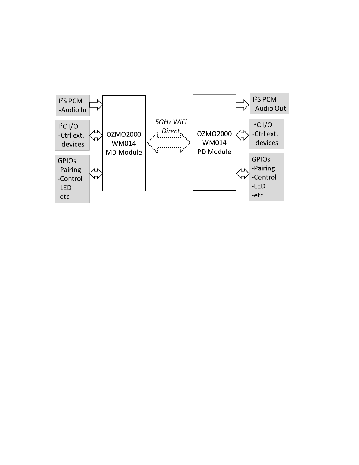
5 Applications information
5.1 Application Diagram
Figure 1 Application Diagram
5.2 Using the module
The WM014 module is designed to operate with customized embedded firmware programmed
into the module by Ozmo Devices which controls the functioning of the radio and the various
interfaces.
The General Purpose Input-Output pins (referred to as AIO or GPIO pins) are configured and
monitored by the firmware.
Depending on the programmed functionality, the module will send data over the wireless link
corresponding to the inputs received on the AIO pins, or will output digital signals from the AIO
pins based on data received over the wireless link.
Ozmo application engineers will work with customers to define the desired Input-Output behavior
and develop the customized firmware to achieve the desired digital input-output behavior. This
has no effect on the radio operation which is defined by low-level firmware and hardware and
always operates in accordance with FCC and Wi-Fi standards. The custom aspects of the
firmware only affect the formatting and timing of the back-end digital I/O functions.
© 2012 Ozmo, Inc. Portions may be covered by one or more of U.S. Patents No. 8,102,871
8,089,982 7,701,271 B1 and 7,826,408 B1. U.S. and foreign patents pending.
Page 3 of 11
OZMO2000WM014 Module User Guide
Pin #
MD Module Pin
name
MD Pin
Description
PD Module Pin
name
PD Pin
Description
1
VBATT
Power supply
VBATT
Power supply
2
GND
GND
3
NC
NC 4 NC
NC 5 NC
NC 6 NC
NC
7
/RESET
Ozmo chip
reset
/RESET
Ozmo chip
reset 8 NC
NC 9 NC
NC
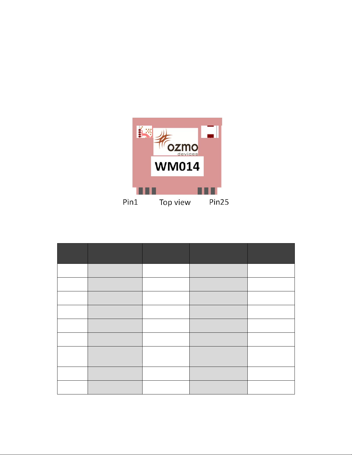
6 Pinout / Pin Description
6.1 Module Pinout
The table below described the pinout and pin descriptions of the module in the default
configuration. Pins are numbered 1 to 25 beginning on the left looking at the module from above
with the antenna end oriented upward and the row of pins at the bottom
Figure 2 Module Pinout (Top View)
© 2012 Ozmo, Inc. Portions may be covered by one or more of U.S. Patents No. 8,102,871
8,089,982 7,701,271 B1 and 7,826,408 B1. U.S. and foreign patents pending.
Page 4 of 11

OZMO2000WM014 Module User Guide
Pin #
MD Module Pin
name
MD Pin
Description
PD Module Pin
name
PD Pin
Description
10
AIO04 (SDA)
I2C Data
AIO4 (SDA)
I2C Data
11
AIO03 (SCL)
I2C Clock
AIO3 (SCL)
I2C Clock
12
AIO0 (LED1)
GPIO 16mA
AIO0 (LED1)
GPIO 16mA
13
AIO01 (LED2)
GPIO 16mA
AIO1 (LED2)
GPIO 16mA
14
AIO07 (I:Pair)
Input from
pairing button
on Master
system, initiates
pairing
procedure.
AIO14 (O:DAC
Reset)
Output to
control
peripheral
function such
as Reset the
DAC
15
AIO13
GPIO
AIO13
GPIO
16
AUDIOCLK
Audio clock
output
AUDIOCLK
Audio clock
output
17
NC
AIO07 (O:MUTE)
Output to
control a
Peripheral
function (such
as mute the
amplifier)
18
AIO15 (I:GPIO)
GPIO
AIO15 (O:/STBY)
Output to
control a
Peripheral
function (such
as place codec
in standby)
19
AIO12 (FSYNC)
Audio In Frame
Sync (I2S
Slave)
AIO9 (FSYNC)
Audio Out
Frame Sync
(I2S Master)
20
AIO14
(I:/ADCSTBY)
Input indicating
system status
such as power
state
NC
21
GND
GND
22
AIO11 (I:PCMIN)
Audio data
input
AIO10
(O:PCMOUT)
Audio data
output
23
AIO8 (I:PCMCLK)
Audio clock
AIO8 (I:PCMCLK)
Audio clock
© 2012 Ozmo, Inc. Portions may be covered by one or more of U.S. Patents No. 8,102,871
8,089,982 7,701,271 B1 and 7,826,408 B1. U.S. and foreign patents pending.
Page 5 of 11

OZMO2000WM014 Module User Guide
Pin #
MD Module Pin
name
MD Pin
Description
PD Module Pin
name
PD Pin
Description
24
GND
GND
25
NC
AIO12 (I:PAIRING/)
Input from
pairing button
on Peripheral
Parameter
Min
Max
Units
Storage temperature
-40
+125
°C
Supply voltage: V
BATT
-0.3
3.6 V GND
-0.3
0.3 V Supply voltage: Digital I/O pins
-0.3
VBATT + 0.3
V
RF Input Power
+10
dBm
Parameter
Min
Typ
Max
Units
Operating temperature
0 +70
°C
Supply voltage: V
BATT
(1)
2.7 3.6
V
GND
0
V
Figure 3 Module Pinout and Pin Descriptions
7 Electrical Characteristics
7.1 Absolute Maximum Ratings
Note: Supply voltage is dependent on ordering option. The on-module flash memory chip can be
either a low-voltage or high-voltage type. The default option is for the high voltage type, supply
voltage 2.7 to 3.6V.
7.2 Recommended Operating Conditions
(1)
Additional limitations may apply. See ordering information for more detail.
© 2012 Ozmo, Inc. Portions may be covered by one or more of U.S. Patents No. 8,102,871
8,089,982 7,701,271 B1 and 7,826,408 B1. U.S. and foreign patents pending.
Page 6 of 11

OZMO2000WM014 Module User Guide
Parameter
Conditions
Min
Typ
Max
Units
VIL, input logic low
1.8 < V
BATT
< 1.95
- 0.3V
BATT
V
VIH, input logic high
1.8 < V
BATT
< 1.95
0.7V
BATT
- V
ΔV, input hysteresis
0.4 V
II, input resistance
Pull-up resistor to V
BATT
42 KΩ
VOL, output logic low
I
OL
= 8 mA (AIO[15:3],
TDO, TSTSEL1, AUXO
0.2 V
BATT
V
VOL, output logic low
I
OL
=16 mA (AIO[2:0])
0.2 V
BATT
V
VOH, output logic high
I
OL
= 8 mA (AIO[15:03,
TDO, AUX0)
0.8 V
BATT
V
VOH, output logic high
I
OL
= 16 mA (AIO[2:0])
0.8 V
BATT
V
IOZ, output tri-state current
0.0 V < V0 < 3.6 V
-10 10
μA
CI, input capacitance
5 pF
CIO, input / output
capacitance
5 pF
7.3 Terminal Characteristics
7.4 Radio Characteristics
7.4.1 Radio Frequencies
This module operates on standard Wi-Fi channels within the 5.15GHz to 5.825GHz bands (limited
to 5180-5240MHz and 5745-5825MHz for operation in the US). Ozmo Devices will program the
module with firmware which automatically selects the channel according to the designated
application requirements established with the customer.
7.4.2 Transmitter
The WM014 module is designed to operate at firmware-controlled transmit power power levels.
The module has been FCC certified at the maximum transmit power settings of +5 dBm
(5.150GHz band) and +1 dBm (5.8GHz band). Firmware may be provided to customers which
configures the device at lower transmit power levels to achieve longer battery life, but it is not
possible to operate this module at any higher power levels than those used during the certification
testing.
© 2012 Ozmo, Inc. Portions may be covered by one or more of U.S. Patents No. 8,102,871
8,089,982 7,701,271 B1 and 7,826,408 B1. U.S. and foreign patents pending.
Page 7 of 11

OZMO2000WM014 Module User Guide
36.3 mm
7.5 ESD Caution Notice
ESD (Electrostatic Discharge) can damage this device. Ozmo, Inc. recommends that all
integrated circuits be handled and stored using appropriate ESD precautions. Failure to observe
proper procedures can cause ESD damage ranging from performance degradation to complete
device failure.
8 Module Floorplan
The diagram below shows the floorplan and dimensions of the OZMO2000WM014 Wireless
Module.
Figure 4 Floorplan of the OZMO2000WM014 Wireless Module
The WM014 module is designed to be mounted to the end-equipment printed circuit board (pcb)
either as a card inserted in a slot or laid flat and soldered as a surface mount component. In the
latter case standard surface-mount technology (SMT) circuit construction procedures should be
followed. For inserting in a slot the pcb is 0.045” thick so the slot should be sized accordingly.
9 Ordering Information
The OZMO2000WM014 wireless module is made available in the following options:
© 2012 Ozmo, Inc. Portions may be covered by one or more of U.S. Patents No. 8,102,871
8,089,982 7,701,271 B1 and 7,826,408 B1. U.S. and foreign patents pending.
Page 8 of 11

OZMO2000WM014 Module User Guide
Order number
Description
OZMO2000WM014-AMH-1321
WM014 Master Device(MD) module: (intended for the
master device such as audio base station or TV Soundbar).
Single pcb trace antenna integral to the module pcb, referred
to as “WM014A1”
OZMO2000WM014-APH-2321
WM014 Peripheral Device(PD) module: (intended for the
peripheral device such as cordless headphones or wireless
sub-woofer)
Dual pcb antenna, referred to as “WM014A2”
Contact your Ozmo sales representative or FAE with further questions or to confirm availability.
10 Regulatory notes
Federal Communication Commission Interference Statement
This equipment has been tested and found to comply with the limits for a Class B digital device,
pursuant to Part 15 of the FCC Rules. These limits are designed to provide reasonable protection
against harmful interference in a residential installation. This equipment generates uses and can
radiate radio frequency energy and, if not installed and used in accordance with the instructions,
may cause harmful interference to radio communications. However, there is no guarantee that
interference will not occur in a particular installation. If this equipment does cause harmful
interference to radio or television reception, which can be determined by turning the equipment
off and on, the user is encouraged to try to correct the interference by one of the following
measures:
- Reorient or relocate the receiving antenna by moving the end equipment.
- Increase the separation between the equipment and receiver.
- Connect the equipment into an outlet on a circuit different from that to which the receiver is
connected.
- Consult the dealer or an experienced radio/TV technician for help.
FCC Caution: To assure continued compliance, (example - use only shielded interface cables
when connecting to computer or peripheral devices). Any changes or modifications not expressly
approved by the party responsible for compliance could void the user's authority to operate this
equipment.
This device complies with Part 15 of the FCC Rules. Operation is subject to the following two
conditions: (1) This device may not cause harmful interference, and (2) this device must accept
any interference received, including interference that may cause undesired operation.
IMPORTANT NOTE:
FCC & IC Radiation Exposure Statement:
© 2012 Ozmo, Inc. Portions may be covered by one or more of U.S. Patents No. 8,102,871
8,089,982 7,701,271 B1 and 7,826,408 B1. U.S. and foreign patents pending.
Page 9 of 11

OZMO2000WM014 Module User Guide
This equipment complies with FCC & IC radiation exposure limits set forth for an uncontrolled
environment.
This transmitter must not be co-located or operating in conjunction with any other antenna or
transmitter. This device is intended only for OEM integrators under the following conditions:
- The transmitter module may not be co-located with any other transmitter or antenna.
As long as the condition above is met, further transmitter test will not be required. However, The
OEM integrator is still responsible for testing their end-product for any additional compliance
requirements required with this module installed (for example, digital device emissions, PC
peripheral requirements, etc.).
IMPORTANT NOTE: In the event that these conditions cannot be met (for example certain laptop
configurations or co-location with another transmitter), then the FCC & IC authorizations are no
longer considered valid and the FCC & IC IDs cannot be used on the final product. In these
circumstances, the OEM integrator will be responsible for re-evaluating the end product (including
the transmitter) and obtaining separate FCC & IC authorizations.
Indoor usage for 5.2GHz
Important note:
Section 15.407(e) of the FCC Rules states that 5.15 – 5.25 GHZ band UNII devices are restricted
to indoor operations.
If the device is configured for those frequencies, the usage of the device must be restricted to
indoor applications.
End Product Labeling
The final end product must be labeled in a visible area with the corresponding FCC ID number.
Similar to: “Contains Transmitter Module FCC ID: EFU-OZMO-WM014-A2”
Manual Information That Must be Included
The user’s manual for end users must include the following information in a prominent location.
Warning: modifications of the product not approved by the manufacturer can void the
user’s authority to operate the device
The end product using this module must be labeled with the FCC 2part statement
“This device complies with FCC Part 15 of the FCC Rules. Operation is subject to the
following two conditions: (1) this device may not cause harmful interference, and (2) this
device must accept any interference received, including interference that may cause
undesired operation.”
This statement can be placed in the user’s manual if the product is too small.
10.1 FCC ID
This module product has been tested to meet FCC requirements for unlicensed devices and the
FCC ID is: EFU-OZMO-WM014-A2
© 2012 Ozmo, Inc. Portions may be covered by one or more of U.S. Patents No. 8,102,871
8,089,982 7,701,271 B1 and 7,826,408 B1. U.S. and foreign patents pending.
Page 10 of 11

OZMO2000WM014 Module User Guide
Example label:
Since this module will be embedded inside other equipment such as consumer audio products, or
peripherals like game controllers, that equipment should be marked with a label as follows:
“Contains Transmitter Module FCC ID: EFU-OZMO-WM014-A2”
Document revision history:
1.0 7/2/2012 Initial release
1.1 7/18/2012 Updated part numbers, misc edits
1.2 7/30/2012 Corrected typos
© 2012 Ozmo, Inc. Portions may be covered by one or more of U.S. Patents No. 8,102,871
8,089,982 7,701,271 B1 and 7,826,408 B1. U.S. and foreign patents pending.
Page 11 of 11
 Loading...