

OXFORD OXFW900-TQ-A Datasheet

Oxford Semiconductor Ltd.
OXFW900
IEEE1394 to ATA/ATAPI Native Bridge
FEATURES
• S400 compliant 1394-1995 Link and Transaction
layers
• Compatible with 1394-1995 and 1394A Phys.
• Buffer Manager with max. RAM bandwidth of
800Mbps
• Microsoft Win98-Second Edition, Win2000 and Apple
MacOS 8.5 generic driver support
• SBP-2 Target Revision 4 compliant interface
• Fully ATA-4 compliant (see T13-1153D)
• Sustained IDE transfer rate of 25 Mbytes per second,
Peak transfer rate of 50Mbytes per second.
• Supports PIO modes 0 to 4, DMA modes 0 to 2 and
Ultra DMA modes 0 to 2
• Integrated 32-bit RISC processor (ARM7TDMI) with
on-chip scratch RAM
DESCRIPTION
The OXFW900 is a high-performance 1394 to
ATA/ATAPI (IDE) native bridge with an integrated target
Serial Bus Protocol (SBP-2 ) controller. By supporting
the SBP-2 protocol, the device can use generic SBP-2
drivers available in the Microsoft Windows 98SE, Microsoft
Windows 2000, Microsoft Millennium and Apple MacOS
operating systems.
The device is ideally suited for smart-cable or tailgate
interface applications for removable-media drives, compact
flash card readers, CD-ROM, CD-R, CD-RW, DVD-ROM,
DVD-RAM and hard disk drives, allowing IDE drives to be
connected to a 1394 serial bus in a plug-and-play fashion.
Both ATA and ATAPI devices are supported using the
same firmware.
This highly integrated device offers a three-chip solution to
native bridge applications using an external 1394 PHY and
Flash ROM. A slow 32Kx8 Flash ROM (up to 120ns) is
sufficient for most optical media applications. For
applications that need a sustained data rate in excess of
10Mbytes per second, for example high performance disk
drives, an 8-bit 50ns FLASH or faster is recommended.
The device is compatible with both 1394-1995 and 1394A
PHYs.
The LINK controller complies with S400 1394-1995
specification. The 1394 transaction layer and SBP-2
protocol is implemented using a combination of the
ARM7TDMI (low-power 32-bit RISC processor), an ORB
(Operational Request Block) hardware co-processor and a
high performance buffer manager.
69 Milton Park, Abingdon, Oxon, OX14 4RX, UK
Tel: +44 (0)1235 824900 Fax: +44(0)1235 821141
Data Sheet
• ORB co-processor to accelerate translation of ORBs
to ATAPI commands
• Supports ORB chaining for increased performance
• High performance ATA command translation in
firmware using Reduced Block Command (RBC) set
• Optional External Serial ROM interface for
configuration data, user serial number, etc.
• Blank Flash memory programming feature via 1394
bus
• 3.3 Volts operation
• Low Power CMOS
• Firmware and Flash Programming Utilities supplied by
Oxford Semiconductor
• ultra-thin 128-TQFP package (14mm x 14mm x 1mm )
The Buffer Manager has a RAM bandwidth of 800Mbps. It
provides storage for 1394 and ATA/ATAPI packets,
automatically storing them and passing them to the
appropriate destinations, without any intervention from the
processor. It also provides storage and manages the
sequencing of ORB fetching to reduce latency and improve
data throughput.
The configuration data including the IEEE OUI
(Organisational Unique Identifier) and device serial number
is stored in the Flash ROM which may be uploaded from
the 1394 bus, even when blank. The device also facilitates
firmware uploads from the 1394 bus.
The ORB co-processor translates ORBs as defined in the
SBP-2 protocol into ATA/ATAPI commands, and
automatically stores error/status messages at an address
specified by the host.
Concurrent operation of the ATA/ATAPI and 1394
interfaces are facilitated using the high throughput Buffer
Manager where LINK, ATAPI manager and ARM7TDMI
can perform interleaved accesses to the on-chip RAM
buffer. The high performance processor ensures that no
significant latency is incurred. The ATA command
translation is performed in firmware to meet RBC (Reduced
Block Commands) standard, T10-1228D. The ATA/ATAPI
Manager supports PIO modes 0 to 4, DMA modes 0 to 2
and Ultra DMA mode 0 to 2 and provides the interface to
the IDE bus. It is compliant with T13-1153D, ATA-4
specification.
OXFW900 Data Sheet Revision 1.0 – Nov 1999
Oxford Semiconductor 1999
Part No. OXFW900-TQ-A

OXFW900
OXFORD SEMICONDUCTOR LTD.
CONTENTS
FEATURES..........................................................................................................................................................1
DESCRIPTION.....................................................................................................................................................1
CONTENTS..........................................................................................................................................................2
1 BLOCK DIAGRAM ......................................................................................................................................3
2 PIN INFORMATION.....................................................................................................................................4
3 PIN DESCRIPTIONS...................................................................................................................................5
4 OPERATING CONDITIONS........................................................................................................................7
5 DC ELECTRICAL CHARACTERISTICS....................................................................................................7
5.1 I/O BUFFERS..........................................................................................................................................................7
6 AC ELECTRICAL CHARACTERISTICS....................................................................................................8
6.1 IDE INTERFACE.....................................................................................................................................................8
6.2 1394 LINK-PHY INTERFACE................................................................................................................................11
6.3 EXTERNAL PROCESSOR INTERFACE................................................................................................................12
7 TIMING WAVEFORMS..............................................................................................................................13
8 PACKAGE INFORMATION.......................................................................................................................27
9 ORDERING INFORMATION.....................................................................................................................28
NOTES...............................................................................................................................................................29
CONTACT DETAILS.........................................................................................................................................30
DISCLAIMER.....................................................................................................................................................30
Data Sheet Revision 1.0 Page 2
OXFW900
OXFORD SEMICONDUCTOR LTD.
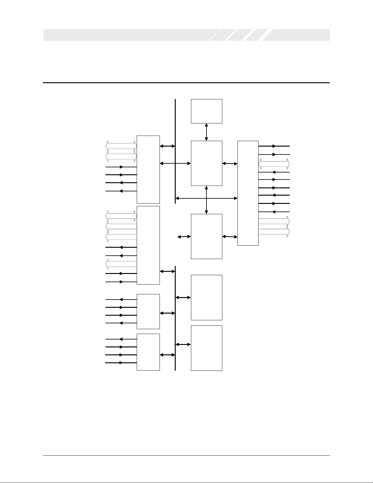
1 BLOCK DIAGRAM
Buffer RAM
PD[7:0]
CTL[1:0]
PHY_CLK
LINK_ON
LPS
LREQ
D[15:0]
A[16:0]
CS#[3:0]
OE#
WE#
BWE#[1:0]
WIDTH16
INT#
XTALO
XTALI
CKIN
CKOUT
Link-Phy
interface
External
ROM
interface
Clock
generator
RAM
Manager
ORB Co-
processor
Internal ARM7TDMI bus
ARM7TDMI
ATA/
ATAPI
manager
IDE_OE#
RTS[3:0]#
ID[15:0]
DMARQ
DIOW#
DIOR#
IORDY
DMACK#
INTRQ#
IA[2:0]
IDE_CS#[2:0]
EE_DO
Data Sheet Revision 1.0 Page 3
EE_DI
EE_CS
EEPROM
interfaceEE_CK
SCRATCH
RAM
Figure 1: OXFW900 Block Diagram
OXFW900
OXFORD SEMICONDUCTOR LTD.
RESET#
2 PIN INFORMATION
INTRQ
DMACK#
VDD
GND
IORDY
DIOR#
DIOW#
DMARQ
VDD
GND
ID15
ID0
VDD
GND
ID14
ID1
ID13
ID2
ID12
ID3
5VBIAS
GND
ID11
ID4
ID10
ID5
ID9
ID6
GND
GND
ID8
ID7
IA1
IA0
IA2
ICS0#
ICS1#
LINKON
LPS
PD7
PD6
GND
GND
PD5
PD4
PD3
PD2
5VBIAS
CKOUT
VDD
PD1
PD0
CTL1
CTL0
GND
PHYCLK
VDD
LREQ
FORCE#
TEST0
TEST1
GPO1
GPO2
GPO3
96959493929190898887868584838281807877767574737271706968676665
97
98
99
100
101
102
103
104
105
106
107
108
109
110
111
112
113
114
115
116
117
OXFW900-TQ-A
118
119
120
121
122
123
124
125
126
127
128
79
64
63
62
61
60
59
58
57
56
55
54
53
52
51
50
49
48
47
46
45
44
43
42
41
40
39
38
37
36
35
34
33
IRESET
IDE_OE#
WIDTH16
INT#
A0
VDD
XTLO
XTLI
CKIN
GND
A1
A2
A3
A4
A5
A6
A7
VDD
GND
A8
A9
A10
A11
A12
A13
GND
5VBIAS
A14
A15
A16
WE#
BWR0#
Data Sheet Revision 1.0 Page 4
12345678910111213141516171920212223242526272829303132
GPI
D15
D14
D13
D12
D11
D10
GND
D9D8D7D6D5
5VBIAS
D4
VDD
GND
18
D2D1D0
D3
GND
VDD
CS3#
CS2#
VDD
GND
CS1#
CS0#
OE#
Figure 2: Pinout (package = 128 TQFP)
BWR#
OXFW900
OXFORD SEMICONDUCTOR LTD.
3 PIN DESCRIPTIONS
1394 PHY-LINK interface Dir1 Name Description
104, 105, 108, 109, 110, 111, 115,
116
117,118 I/O CTL[1:0] Phy-Link Control Bus
120 I PHYCLK 49.152 MHz clock sourced by PHY
122 O LREQ Link Request
102 IU LINKON Requests link to power up when in a low power mode
103 O LPS Indicates to phy that link is powered and ready
ARM external interface
2, 3, 4, 5, 6, 7, 10, 11, 12, 13, 14,
15, 18, 19, 20, 21
35, 36, 37, 40, 41, 42, 43, 44, 45,
48, 49, 50, 51, 52, 53, 54, 60
25, 26, 29, 30 T_O CS#[3:0] ARM external chip selects. CS0# is always used for program
31 T_O OE# ARM external output enable. Active when reading data from
32, 33 T_O BWR#[1:0] Byte Write enables. For future expansion
34 T_O WE# Write Enable. Active when writing to external devices
62 ID WIDTH16 ‘1’ = 16 bit external ROM ‘0’ = 8 bit external ROM
61 T_IU INT# External ARM interrupt
IDE interface
65, 66, 69, 70, 71, 72, 73, 74, 77,
78, 79, 80, 81, 82, 85, 86
97, 98, 99 T_O IA[2:0] IDE address bus
100, 101 T_O ICS#[1:0] IDE chip select. Selects IDE drive 0 or 1
63 T_O IDE_OE#[ IDE output enable. Only used when external buffering is
64 T_O IRESET IDE interface reset
89 T_I DMARQ
90 T_O DIOW# IDE interface write strobe
91 T_O DIOR# IDE interface read strobe
92 T_O IORDY
95 T_O DMACK#
96 T_I INTRQ
EEPROM interface
128 O GPO3 General Purpose Output 3
126 O GPO1 General Purpose Output 1
1 IU GPI General Purpose Input
127 O GPO2 General Purpose Output 2
Miscellaneous Pins
57 I XTLI Crystal Oscillator input. 24.576 MHz crystal required. If a
58 O XTLO Crystal Oscillator output. IMPORTANT – See Application
I/O PD[7:0] Phy-Link Data Bus
T_I/O D[15:0] ARM external data bus
T_O A[16:0] ARM external address bus
ROM.
external devices including program ROM
(pulldown)
T_I/O ID[15:0] IDE data bus
required to drive IDE data bus
clock module is used rather than a crystal then this input
must be tied high for the OXFW900 to operate, and the clock
module output connected to the CKIN pin. IMPORTANT See Application Notes regarding clocking
Notes regarding clocking.
Data Sheet Revision 1.0 Page 5
OXFW900
OXFORD SEMICONDUCTOR LTD.
56 I CKIN Direct clock input. Used in conjunction with an external
crystal oscillator of 24.576MHz. If a crystal is connected to
XTLI and XTLO this input must be tied low for the OXFW900
to operate. Mark space ratio of crystal oscillator must be
45:55 or better. IMPORTANT – Please refer to Application
Notes regarding clocking
23 IU RESET# Global reset for the OXFW900. Active Low.
113 T_O CKOUT Clock output. 24.576 MHz clock output. IMPORTANT –
Please refer to Application Notes regarding clocking
123 IU FORCE# This input is used to allow the OXFW900 to reprogram a
flash which has been loaded with a bad program. A bad
program is defined as one that does not have the correct
interlocking mechanism for reprogramming flash. This pin
forces the ARM watchdog timer to trigger thus allowing the
flash to be reprogrammed over the 1394 bus as if the flash
were blank.
124, 125 IU TEST[1:0] ‘11’ = NORMAL OPERATION. These pins have internal
pullup resistors and must be left unconnected. Other settings
are for foundry test purposes only.
Power and ground2
28, 47, 94, 114 3V3 3.3V AC VDD Supplies power to output buffers in switching (AC) state
17, 24, 59, 84, 88, 121 3V3 3.3V DC VDD Power supply. Supplies power to core logic, input buffers
and output buffers in steady state
9, 38, 76, 112 5V 5V BIAS VDD Supplies 5V reference bias to all 5V tolerant I/O. All four
MUST be connected to 5V rail.
8, 27, 46, 67, 75, 93, 106 G AC GND Supplies GND to output buffers in switching (AC) state
16, 22, 39, 55, 68, 83, 87, 107, 119 G DC GND Ground (0 volts). Supplies GND to core logic, input buffers
and output buffers in steady state
Table 1: Pin Descriptions
Note 1: Direction key:
I Input
IU Input with internal pull-up
ID Input with external pull-down
O Output
I/O Bi-directional
T_I 5V tolerant input
Note 2: Power & Ground
There are two GND and three VDD rails internally. One set of rails supply power and ground to output buffers while in switching
state (called AC power) and another rail supply the core logic, input buffers and output buffers in steady-state (called DC rail). A
third rail provides 5V bias voltage to 5V tolerant IO.
The rails are not connected internally. This precaution reduces the effects of simultaneous switching outputs and undesirable RF
radiation from the chip.
T_O 5V tolerant output
T_I/O 5V tolerant bi-directional
G Ground
3V3 3.3V power
5V 5V bias power
Data Sheet Revision 1.0 Page 6
OXFW900
OXFORD SEMICONDUCTOR LTD.
Configuration & Operation
4 OPERATING CONDITIONS
Symbol Parameter Min Max Units
VDD DC supply voltage -0.3 4.6 V
VIN DC input voltage -0.3 VDD + 0.3 V
IIN DC input current +/- 10 mA
T
Storage temperature -40 125
STG
Table 2: Absolute maximum ratings
Symbol Parameter Min Max Units
VDD DC supply voltage 3.0 3.6 V
VBB 5V PMOS bulk bias 4.75 5.25 V
TC Temperature 0 70
Table 3: Recommended operating conditions
5 DC ELECTRICAL CHARACTERISTICS
°C
°C
5.1 I/O Buffers
Symbol Parameter Condition Min Max Units
VDD Supply voltage Commercial 3.0 3.6 V
V
VIL Input low voltage CMOS Interface 1
CIL Cap of input buffers 5.0 pF
COL Cap of output buffers 10.0 pF
IIH Input high leakage current Vin = VDD -10 10
IIL Input low leakage current Vin = VSS -10 10
VOH Output high voltage
VOH Output high voltage IOH = -1mA to –24mA 2.4 V
VOL Output low voltage
VOL Output low voltage IOL = 1mA to 24mA 0.4 V
IOZ 3-state output leakage current -10 10
Symbol Parameter Condition Typical Max Units
ICC
Input high voltage CMOS Interface
IH
Operating supply current in
normal mode
Operating supply current in
Power-down mode
0.7 x Vdd
CMOS Schmitt trig
2.1
0.3 x Vdd
CMOS Schmitt trig
IOH = -1 µA
IOL = 1 µA
VDD – 0.05
0.05 V
0.8
V
V
V
µA
µA
µA
mA
Data Sheet Revision 1.0 Page 7
Table 4: Characteristics of OXFW900 I/O buffers
OXFW900
OXFORD SEMICONDUCTOR LTD.
6 AC ELECTRICAL CHARACTERISTICS
6.1 IDE interface
Symbol Parameter Mode 0 Mode 1 Mode 2 Mode 3 Mode 4 Units
t0 Cycle Time 600 400 360 200 120 ns
t1 Address Valid to DIOR# / DIOW#
setup
t2 DIOR# / DIOW# pulse width 320 320 320 80 80 ns
t2i DIOR# / DIOW# recovery time - - - 80 40 ns
t3 DIOW# data setup (min ) 60 45 30 30 20 ns
t4 DIOW# data hold 40 40 40 40 40 ns
t5 DIOR# data setup ( min ) 50 35 20 20 20 ns
t6 DIOR# data hold ( min ) 5 5 5 5 5 ns
t6z DIOR# data tristate (max ) 30 30 30 30 30 ns
t9 DIOR# / DIOW# to address valid
hold
tRD Read Data Valid to IORDY active if
IORDY initially low after tA
tA IORDY Setup time 35 35 35 35 35 ns
tB IORDY Pulse Width ( max ) 1250 1250 1250 1250 1250 ns
tA IORDY assertion to release 5 5 5 5 5 ns
80 80 40 40 40 ns
40 40 40 40 40 ns
0 0 0 0 0 ns
Table 5: OXFW900 IDE PIO / Register Transfers
Data Sheet Revision 1.0 Page 8

OXFW900
OXFORD SEMICONDUCTOR LTD.
Symbol Parameter Mode 0 Mode 1 Mode 2 Units
t0 Cycle time 480 160 120 ns
tD DIOR# / DIOW# 240 80 80 ns
tE DIOR# data access ( max ) 150 60 50 ns
tF DIOR# data hold ( min ) 5 5 5 ns
tG DIOR# / DIOW# data setup 100 30 20 ns
tH DIOW# data hold 20 15 10 ns
tI DMACK to DIOR# / DIOW# setup ( min ) 0 0 0 ns
tJ DIOR# / DIOW# to DMACK hold ( min ) 20 5 5 ns
tKr DIOR# negated pulse width 80 80 40 ns
tKw DIOW# negated pulse width 240 80 40 ns
tLr DIOR# to DMARQ delay ( max ) 120 40 35 ns
tLw DIOW# to DMARQ delay ( max ) 40 40 35 ns
tM IDCS[1:0] valid to DIOR# / DIOW# 80 40 40 ns
tN IDCS[1:0] hold 40 40 40 ns
tZ DMACK to tristate ( max ) 20 25 25 ns
Table 6: OXFW900 Multiword DMA timings
Data Sheet Revision 1.0 Page 9
 Loading...