

OXFORD OXCB950 Datasheet

Oxford Semiconductor Ltd.
A
OXCB950
Integrated High Performance UART
FEATURE
• Single 16C950 High performance UART channel
• Cardbus/PCI compliant, single-function target
controller. Fully compliant to PC Card Standard 7.0*,
and PCI Bus Specification 2.2, Power Management
1.0.
• Function access to pre-configure UART prior to
handover to generic device drivers.
• UART fully software compatible with 16C550-type
devices.
• Baud rates up to 15Mbps in asynchronous mode and
60Mbps in external 1x clock mode
• 128-byte deep FIFO per transmitter and receiver
• Flexible clock prescaler from 1 to 31.875
• Automated in-band flow control using programmable
Xon/Xoff in both directions
• Automated out-of-band flow control using CTS#/RTS#
and/or DSR#/DTR#
* Compliance to PC Card Standard 7.1 requires small external circuitry.
Cardbus / PCI interface
• Arbitrary trigger levels for receiver and transmitter
FIFO interrupts and automatic in-band and out-ofband flow control
• Infra-red (IrDA) receiver and transmitter operation
• 9-bit data framing as well as 5,6,7 and 8
• Global Interrupt Status and readable FIFO levels to
facilitate implementation of efficient device drivers
• Detection of bad data in the receiver FIFO
• Operation via IO or memory mapping.
• 2 Multi-purpose I/O pins which can be configured as
interrupt input or ‘wake-up’ pins
• Auto-detection of optional MicrowireTM based
EEPROM, to reconfigure device.
Autodetected.
• 3.3V operation
• 100 pin TQFP package
DESCRIPTION
The OXCB950 is a single chip UART solution for either
cardbus or PCI-based serial add-in cards. It is a single
function device, offering memory or IO mapped access to
the ultra-high performance OX16C950 UART.
This UART is the fastest available PC-compatible UART,
offering data rates up to 15Mbps and 128-deep transmitter
and receiver FIFOs. The deep FIFOs reduce CPU
overhead and allow utilisation of higher data rates. The
UART is software compatible with the widely used industrystandard 16C550 devices and compatibles, as well as the
OX16C95x family of high performance UARTs. In addition
to increased performance and FIFO size, the UART also
provides the full set of OX16C95x enhanced features
including automated in-band flow control, readable FIFO
levels etc.
A set of local registers is available to enhance device driver
efficiency and reduce interrupt latency. The internal UART
has features such as shadowed FIFO fill levels, an interrupt
source register and Good-Data Status, readable in one
DWORD register visible to logical function0 in IO space
and memory space.
The efficient 32-bit, 33MHz target-only interface is
compliant with both the cardbus sections of the PC CARD
Standard, release 7.0*, and the PCI bus specifications
version 2.2 and version 1.0 of PCI Power Management
Specification.
For full flexibility, all the default register values can be
overwritten using an optional MicrowireTM serial EEPROM.
This EEPROM can also be used to provide function access
to pre-configure the UART into enhanced modes prior to
any cardbus/PCI configuration accesses and before control
is handed to generic device drivers.
25 ParkGate, Milton Park, Abingdon, Oxon, OX14 4SH, UK
Tel: +44 (0)1235 824900 Fax: +44(0)1235 821141
OXCB950 Datasheet 1.1 – November 2000
Oxford Semiconductor 2000
Part No. OXCB950-TQFP-

OXFORD SEMICONDUCTOR LTD.
OXCB950
CONTENTS
1 PERFORMANCE COMPARISON..................................................................................................4
1.1 IMPROVEMENTS OF THE OXCB950 OVER DISCRETE SOLUTIONS:...........................................................................4
2 BLOCK DIAGRAM.......................................................................................................................5
3 PIN INFORMATION .....................................................................................................................6
4 PIN DESCRIPTIONS....................................................................................................................7
5 CONFIGURATION & OPERATION............................................................................................. 11
6 PCI TARGET CONTROLLER ..................................................................................................... 12
6.1 OPERATION........................................................................................................................................................................12
6.2 CONFIGURATION SPACE.................................................................................................................................................13
6.2.1 CARDBUS / PCI CONFIGURATION SPACE REGISTER MAP.....................................................................................13
6.3 ACCESSING THE UART FUNCTION ................................................................................................................................15
6.3.1 CARDBUS/PCI ACCESS TO THE INTERNAL UART....................................................................................................15
6.4 ACCESSING LOCAL CONFIGURATION REGISTERS....................................................................................................16
6.4.1 LOCAL CONFIGURATION AND CONTROL REGISTER ‘LCC’ (OFFSET 0X00).........................................................16
6.4.2 MULTI-PURPOSE I/O CONFIGURATION REGISTER ‘MIC’ (OFFSET 0X04).............................................................17
6.4.3 UART MIRROR REGISTER ‘UMR’ (OFFSET 0X08): ....................................................................................................18
6.4.4 GLOBAL INTERRUPT STATUS AND CONTROL REGISTER ‘GIS’ (OFFSET 0X0C)................................................19
6.5 CARDBUS/ PCI INTERRUPT.............................................................................................................................................20
6.6 CARDBUS/PCI POWER MANAGEMENT..........................................................................................................................21
6.6.1 POWER MANAGEMENT VIA UART/ MIO PINS............................................................................................................21
6.6.2 POWER REPORTING.....................................................................................................................................................22
6.6.3 CARDBUS POWER MANAGEMENT.............................................................................................................................23
6.7 CARDBUS STATUS REGISTERS .....................................................................................................................................24
6.8 CARDBUS TUPLE INFORMATION ...................................................................................................................................26
7 INTERNAL OX16C950 UART..................................................................................................... 27
7.1 OPERATION – MODE SELECTION...................................................................................................................................27
7.1.1 450 MODE.......................................................................................................................................................................27
7.1.2 550 MODE.......................................................................................................................................................................27
7.1.3 750 MODE.......................................................................................................................................................................27
7.1.4 650 MODE.......................................................................................................................................................................27
7.1.5 950 MODE.......................................................................................................................................................................28
7.2 REGISTER DESCRIPTION TABLES .................................................................................................................................29
7.3 RESET CONFIGURATION .................................................................................................................................................33
7.3.1 HARDWARE RESET.......................................................................................................................................................33
7.3.2 SOFTWARE RESET .......................................................................................................................................................33
7.4 TRANSMITTER AND RECEIVER FIFOS...........................................................................................................................34
7.4.1 FIFO CONTROL REGISTER ‘FCR’................................................................................................................................34
7.5 LINE CONTROL & STATUS...............................................................................................................................................35
7.5.1 FALSE START BIT DETECTION....................................................................................................................................35
7.5.2 LINE CONTROL REGISTER ‘LCR’................................................................................................................................35
7.5.3 LINE STATUS REGISTER ‘LSR’....................................................................................................................................36
7.6 INTERRUPTS & SLEEP MODE .........................................................................................................................................37
7.6.1 INTERRUPT ENABLE REGISTER ‘IER’........................................................................................................................37
7.6.2 INTERRUPT STATUS REGISTER ‘ISR’........................................................................................................................38
7.6.3 INTERRUPT DESCRIPTION..........................................................................................................................................38
7.6.4 SLEEP MODE .................................................................................................................................................................39
7.7 MODEM INTERFACE.........................................................................................................................................................39
7.7.1 MODEM CONTROL REGISTER ‘MCR’..........................................................................................................................39
Data Sheet Revision 1.1 Page 2

OXFORD SEMICONDUCTOR LTD.
7.7.2 MODEM STATUS REGISTER ‘MSR’.............................................................................................................................40
7.8 OTHER STANDARD REGISTERS.....................................................................................................................................40
7.8.1 DIVISOR LATCH REGISTERS ‘DLL & DLM’.................................................................................................................40
7.8.2 SCRATCH PAD REGISTER ‘SPR’.................................................................................................................................40
7.9 AUTOMATIC FLOW CONTROL.........................................................................................................................................41
7.9.1 ENHANCED FEATURES REGISTER ‘EFR’...................................................................................................................41
7.9.2 SPECIAL CHARACTER DETECTION............................................................................................................................42
7.9.3 AUTOMATIC IN-BAND FLOW CONTROL.....................................................................................................................42
7.9.4 AUTOMATIC OUT-OF-BAND FLOW CONTROL...........................................................................................................42
7.10 BAUD RATE GENERATION ...............................................................................................................................................43
7.10.1 GENERAL OPERATION .................................................................................................................................................43
7.10.2 CLOCK PRESCALER REGISTER ‘CPR’.......................................................................................................................43
7.10.3 TIMES CLOCK REGISTER ‘TCR’...................................................................................................................................43
7.10.4 EXTERNAL 1X CLOCK MODE.......................................................................................................................................45
7.10.5 CRYSTAL OSCILLATOR CIRCUIT................................................................................................................................45
7.11 ADDITIONAL FEATURES ..................................................................................................................................................45
7.11.1 ADDITIONAL STATUS REGISTER ‘ASR’......................................................................................................................45
7.11.2 FIFO FILL LEVELS ‘TFL & RFL’.....................................................................................................................................46
7.11.3 ADDITIONAL CONTROL REGISTER ‘ACR’..................................................................................................................46
7.11.4 TRANSMITTER TRIGGER LEVEL ‘TTL’........................................................................................................................47
7.11.5 RECEIVER INTERRUPT. TRIGGER LEVEL ‘RTL’........................................................................................................47
7.11.6 FLOW CONTROL LEVELS ‘FCL’ & ‘FCH’......................................................................................................................47
7.11.7 DEVICE IDENTIFICATION REGISTERS .......................................................................................................................47
7.11.8 CLOCK SELECT REGISTER ‘CKS’...............................................................................................................................48
7.11.9 NINE-BIT MODE REGISTER ‘NMR’...............................................................................................................................48
7.11.10 MODEM DISABLE MASK ‘MDM’....................................................................................................................................49
7.11.11 READABLE FCR ‘RFC’...................................................................................................................................................49
7.11.12 GOOD-DATA STATUS REGISTER ‘GDS’ .....................................................................................................................49
7.11.13 DMA STATUS REGISTER ‘DMS’ ...................................................................................................................................50
7.11.14 PORT INDEX REGISTER ‘PIX’.......................................................................................................................................50
7.11.15 CLOCK ALTERATION REGISTER ‘CKA’.......................................................................................................................50
OXCB950
8 SERIAL EEPROM SPECIFICATION ........................................................................................... 51
8.1 EEPROM DATA ORGANISATION.....................................................................................................................................51
8.1.1 ZONE0: HEADER............................................................................................................................................................51
8.1.2 ZONE1 : POWER MANAGEM ENT DATA, DATA_SCALE ZONE ................................................................................. 52
8.1.3 ZONE2: LOCAL CONFIGURATION REGISTER ZONE................................................................................................53
8.1.4 ZONE 3 : CARDBUS INFORMATION STRUCTURE.....................................................................................................53
8.1.5 ZONE4: PCI CONFIGURATION REGISTERS...............................................................................................................54
8.1.6 ZONE5: FUNCTION ACCESS........................................................................................................................................55
9 COMPLIANCE TO PC CAR D STANDARDS, 7.0 AND 7.1............................................................57
10 OPERATING CONDITIONS..................................................................................................... 60
11 DC ELECTRICAL CHARACTERISTICS................................................................................... 61
11.1 NORMAL 3.3V I/O BUFFERS.............................................................................................................................................61
11.2 5.0V TOLERANT I/O BUFFERS ........................................................................................................................................ 61
11.3 DUAL MODE (CARDBUS/PCI) I/O BUFFERS.................................................................................................................62
12 POWER CONSUMPTION MEASUREMENTS........................................................................... 63
12.1 STATIC CURRENT CONSUMPTION.................................................................................................................................63
12.2 CURRENT CONSUMPTION IN APPLICATION.................................................................................................................63
13 TIMING WAVEFORMS............................................................................................................ 64
14 PHYSICAL PACKAGE DETAILS .............................................................................................66
Data Sheet Revision 1.1 Page 3

OXFORD SEMICONDUCTOR LTD.
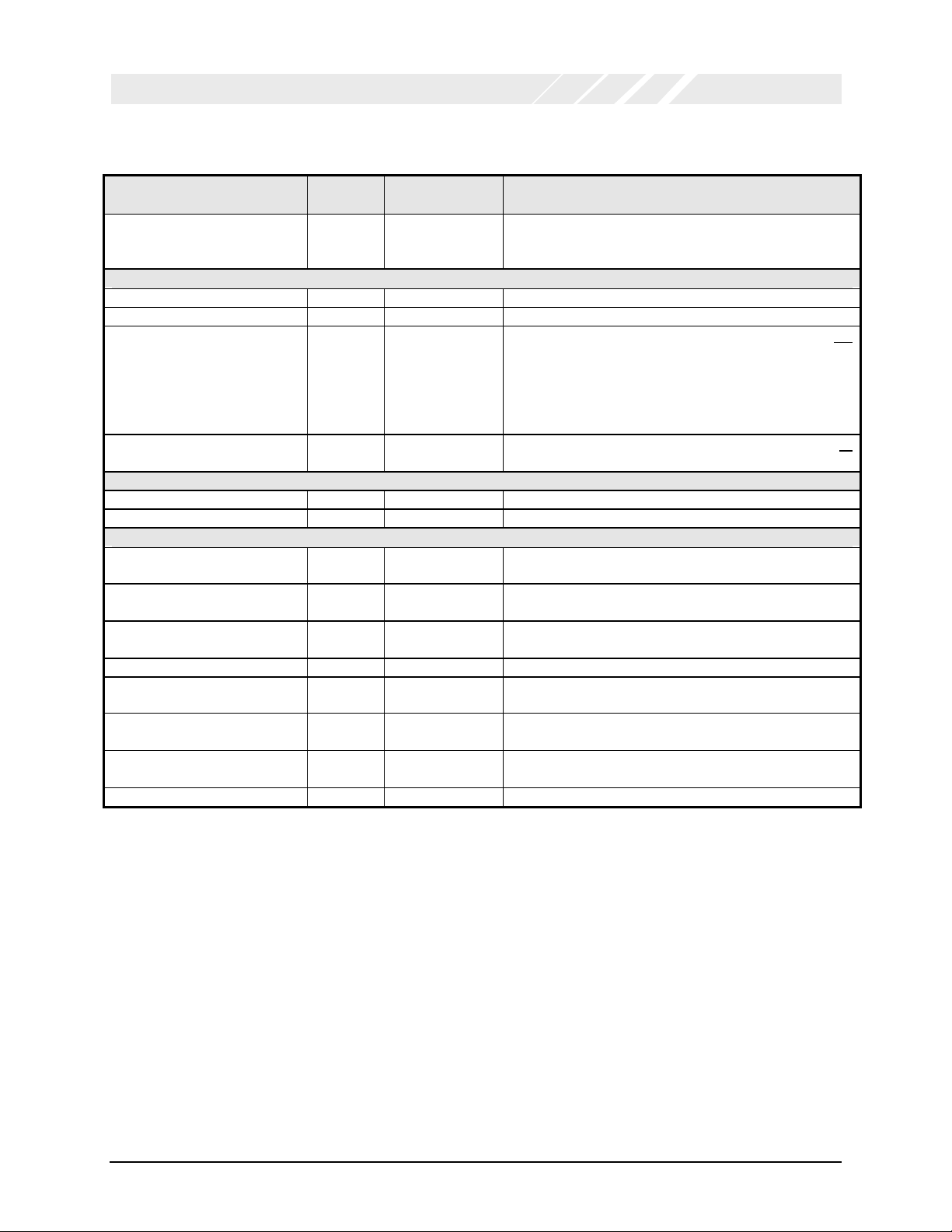
1 PERFORMANCE COMPARISON
Feature OXCB950 16C550 +
Support for PCI Power Management yes no No
Zero wait-state read/write operation yes no No
No. of external interrupt source pins 2 2 2
DWORD access to UART Interrupt Source
Registers & FIFO Levels
Good-Data status yes no No
Full Plug and Play with external EEPROM yes yes Yes
External 1x baud rate clock yes no No
Max baud rate in normal mode 15 Mbps 115 Kbps 1.5 Mbps
Max baud rate in 1x clock mode 60 Mbps n/a n/a
FIFO depth 128 16 64
Sleep mode yes no Yes
Auto Xon/Xoff flow yes no Yes
Auto CTS#/RTS# flow yes no Yes
Auto DSR#/DTR# flow yes no No
No. of Rx interrupt thresholds 128 4 4
No. of Tx interrupt thresholds 128 1 4
No. of flow control thresholds 128 n/a 4
Transmitter empty interrupt yes no No
Readable status of flow control yes no No
Readable FIFO levels yes no No
Clock prescaler options 248 n/a 2
Rx/Tx disable yes no No
Software reset yes no No
Device ID yes no No
9-bit data frames yes no No
RS485 buffer enable yes no No
Infra-red (IrDA) yes no Yes
16C650 +
PLX9050
yes no No
PLX9050
OXCB950
Table 1: OXCB950 performance compared with PLX + generic UART combinations in PCI mode
1.1 Improvements of the OXCB950 over discrete solutions:
Improved access timing:
Access to the internal UART requires zero or one PCI wait states. A cardbus/PCI read transaction from the internal UART can
complete within five PCI clock cycles and a write transaction to the internal UART can complete within four PCI clock cycles.
Reduces interrupt latency:
The OXCB950 offers shadowed FIFO levels and Interrupt status registers of the internal UART, as well as general device
interrupt status, to reduce the device driver interrupt latency.
Power management:
The OXCB950 complies with the Cardbus Power Management Specification, given by the PC CARD standard release 7.0/7.1,
the PCI Power Management Specification 1.0 and the PC98/99 Power Management specifications, by offering the extended
capabilities for Power Management and supporting the power states D0, D2 and D3. This achieves significant power savings by
allowing device drivers to power down the cardbus/PCI function and disable the UART channel.
Data Sheet Revision 1.1 Page 4
OXFORD SEMICONDUCTOR LTD.
OXCB950
A ‘wake-up’ event (the ‘power management event’) is requested via the PME# (PCI) or CSYSCHG (cardbus) pins from either of
the power states D2 or D3, by the UART line RI (for power state D3), and any modem line and the Serial Data In (for power state
D2).
Optional EEPROM:
The OXCB950 can be reconfigured from an external Microwire
TM
based EEPROM. However, this is not required in many
applications as default values are provided for typical applications. Features available via the use of the EEPROM include
redefining device ID’s and vendor/sub-vendor ID fields in the PCI header space, cardbus-to-pci mode change, redefining Tuple
Information (relevant to cardbus applications only), and selectively enabling/disabling interrupts, powerdown and wakeup
requests.
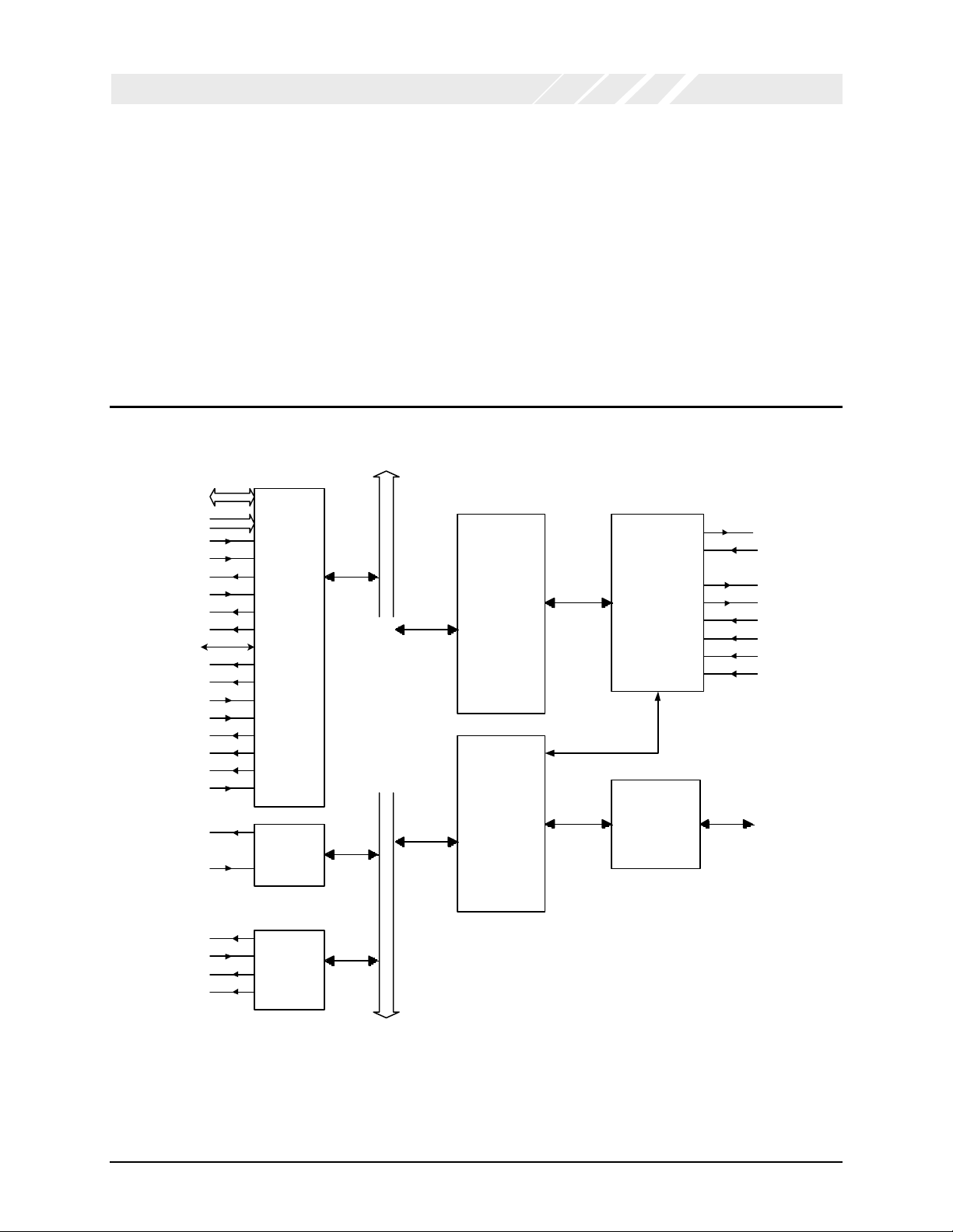
2 BLOCK DIAGRAM
AD[31:0]
C/BE[3:0]
CLK
FRAME#
DEVSEL#
IRDY#
TRDY#
STOP#
PAR
SERR#
PERR#
RST#
IDSEL
INTA#
INTB#
PME#
SLEW_RATE
PCI
3.3V or
CardBus
Interface
Function 0
Internal Data/Control Bus
UART
SOUT
SIN
RTS
DTR
CTS
DSR
DCD
RI
XTALO
Clock &
Interrupt logic
MIO pins
MIO[1:0]
Baud rate
XTALI
EE_DO
EE_DI
EE_CK
EE_CS
Generator
EEPROM
interface
Data Sheet Revision 1.1 Page 5

OXFORD SEMICONDUCTOR LTD.
OXCB950
3 PIN INFORMATION
100 pin TQFP (14mm x 14mm)
AD20
| AD21
| | AD22
| | | Z_SERR
| | | | VDD3OP_CB
| | | | | VSS0P_CB
| | | | | | AD23
| | | | | | | IDSEL
| | | | | | | | Z_CBE3
| | | | | | | | | AD24
| | | | | | | | | | VSS0P_CB
| | | | | | | | | | | VSSOP_CB
| | | | | | | | | | | | VDD3I_CB
| | | | | | | | | | | | | VSSI_CB
| | | | | | | | | | | | | | AD25
| | | | | | | | | | | | | | | AD26
| | | | | | | | | | | | | | | | CSYSCHG
| | | | | | | | | | | | | | | | | AD27
| | | | | | | | | | | | | | | | | | AD28
| | | | | | | | | | | | | | | | | | | VDD3OP_CB
| | | | | | | | | | | | | | | | | | | | VSS0P_CB
| | | | | | | | | | | | | | | | | | | | | AD29
| | | | | | | | | | | | | | | | | | | | | | AD30
| | | | | | | | | | | | | | | | | | | | | | | AD31
| | | | | | | | | | | | | | | | | | | | | | | | Z_PME
| | | | | | | | | | | | | | | | | | | | | | | | |
| | | | | | | | | | | | | | | | | | | | | | | | |
VSS0P_CB -- -- VSS0
AD19 -- -- EXT_DATA_OUT
AD18 -- -- Z_RTS
AD17 -- -- Z_DTR
Z_CBE2 -- -- Z_CTS
VDD3OP_CB -- -- Z_DSR
VSS0P_CB -- -- Z_DCD
Z_FRAME -- -- Z_RI
Z_IRDY -- -- EXT_DATA_IN
Z_TRDY -- -- VDD0
Z_RESET -- -- VSS0
VSSI_CB -- -- VDDIP
PCI_CLK -- -- VDDIP
VDD3I_CB -- -- XTLO
VSSOP_CB -- -- XTLI
VDD3OP_CB -- -- VSSIP
VSS0P_CB -- -- TEST0
Z_DEVSEL -- -- TEST1
Z_CINT -- . -- BUFFER_SLEW_RATE
Z_STOP -- . -- EEPROM_DI
Z_PERR -- . -- EEPROM_DO
VSS0P_CB -- 97 -- EEPROM_CS
PAR -- 98 -- EEPROM_SK
Z_CBE1 -- 99 -- MIO1
AD16 -- 1 2 3 4 5 6 7... -- MIO0
| | | | | | | | | | | | | | | | | | | | | | | | |
| | | | | | | | | | | | | | | | | | | | | | | | |
| | | | | | | | | | | | | | | | | | | | | | | | AD0
| | | | | | | | | | | | | | | | | | | | | | | AD1
| | | | | | | | | | | | | | | | | | | | | | AD2
| | | | | | | | | | | | | | | | | | | | | AD3
| | | | | | | | | | | | | | | | | | | | VDD30P_CB
| | | | | | | | | | | | | | | | | | | VSS0P_CB
| | | | | | | | | | | | | | | | | | AD4
| | | | | | | | | | | | | | | | | AD5
| | | | | | | | | | | | | | | | AD6
| | | | | | | | | | | | | | | AD7
| | | | | | | | | | | | | | Z_CBE0
| | | | | | | | | | | | | VDD3I_CB
| | | | | | | | | | | | VSSI_CB
| | | | | | | | | | | VSS0P_CB
| | | | | | | | | | AD8
| | | | | | | | | AD9
| | | | | | | | AD10
| | | | | | | AD11
| | | | | | VDD30P_CB
| | | | | VSS0P_CB
| | | | AD12
| | | AD13
| | AD14
| VSSOP_CB
AD15
Data Sheet Revision 1.1 Page 6

OXFORD SEMICONDUCTOR LTD.
OXCB950
4 PIN DESCRIPTIONS
Cardbus/PCI bus Pins Dir1 Name Description
52, 53, 54, 57, 58, 60, 61, 66,
69, 73, 74, 75, 77, 78, 79, 100,
1, 3, 4, 5, 8, 9, 10, 11, 16, 17,
18, 19, 22, 23, 24, 25
67, 80, 99, 15 C/P_I C/BE[3:0]# Multiplexed Command/Byte enable.
88 CP_I CLK System clock
83 CP_I FRAME# Cycle Frame1.
93 CP_O DEVSEL# Device Select
84 CP_I IRDY# Initiator ready
85 CP_O TRDY# Target ready
95 CP_O STOP# Target Stop request
98 CP_I/O PAR Parity
72 CP_O SERR# System error
96 CP_I/O PERR# Parity error
68 CP_I IDSEL Initialisation device select
86 CP_I RST# System reset
94 CP_OD INTA# /CINT# Interrupt Pin. For both cardbus and pci applications
59 CP_O CSYSCHG Power management event signal, for Cardbus applications
51 CP_OD PME# Power management event signal, for PCI applications
32 I SLEW_RATE Slew rate control for cardbus/pci outputs
1
For cardbus applications, the pin z_frame requires a pull-up (4k7) on the board. See PC Card Standard 7.0/7.1, section
5.3.3.3.3 “pull-up resistor requirements”.
C/P_I/O AD[31:0] Multiplexed Address/Data bus.
For PCI applications this pin must be connected to the IDSEL
pin on the PCI connector. For cardbus applications, there is
no IDSEL signal, so this pin must be tied to Vdd (3.3v) via a
pull-up on the board. (10K recommended).
This pin must be No-Connect (NC) for PCI applications.
This pin must be No-Connect (NC) for cardbus applications.
For cardbus applications, this must be tied to Vdd on the
board. For PCI applications, this must be tied to Gnd on the
board.
Data Sheet Revision 1.1 Page 7

OXFORD SEMICONDUCTOR LTD.
UART pins Dir1 Name Description
49 T_O EXT_DATA_OUT
42 T_I
44 T_I DCD# Active-low modem data-carrier-detect input
47 T_O
48 T_O RTS# Active-low modem request-to-send output. If automated
46 T_I CTS# Active-low modem clear-to-send input. If automated CTS#
45 T_I
43 T_I
37 O XTLO Crystal oscillator output
36 I XTLI Crystal oscillator input (10MHz – 40 MHz) or external clock
T_I
T_O
T_O
T_I
T_I
IrDA_Out
EXT_DATA_IN
IrDA_In
DTR#
485_En
Tx_Clk_Out
DSR#
Rx_Clk_In
RI#
Tx_Clk_In
OXCB950
UART serial data output
UART IrDA data output when MCR[6] of the corresponding
channel is set in enhanced mode
UART serial data input
UART IrDA data input when IrDA mode is enabled (see
above)
Active-low modem data-terminal-ready output. If automated
DTR# flow control is enabled, the DTR# pin is asserted and
deasserted if the receiver FIFO reaches or falls below the
programmed thresholds, respectively.
In RS485 half-duplex mode, the DTR# pin may be
programmed to reflect the state of the the transmitter empty
bit to automatically control the direction of the RS485
transceiver buffer (see register ACR[4:3])
Transmitter 1x clock (baud rate generator output). For
isochronous applications, the 1x (or Nx) transmitter clock
may be asserted on the DTR# pins (see register CKS[5:4])
RTS# flow control is enabled, the RTS# pin is deasserted
and reasserted whenever the receiver FIFO reaches or falls
below the programmed thresholds, respectively.
flow control is enabled, upon deassertion of the CTS# pin,
the transmitter will complete the current character and enter
the idle mode until the CTS# pin is reasserted. Note: flow
control characters are transmitted regardless of the state of
the CTS# pin.
Active-low modem data-set-ready input. If automated DSR#
flow control is enabled, upon deassertion of the DSR# pin,
the transmitter will complete the current character and enter
the idle mode until the DSR# pin is reasserted. Note: flow
control characters are transmitted regardless of the state of
the DSR# pin
External receiver clock for isochronous applications. The
Rx_Clk_In is selected when CKS[1:0] = ‘01’.
Active-low modem Ring-Indicator input
External transmitter clock. This clock can be used by the
transmitter (and indirectly by the receiver) when CKS[6]=’1’.
pin. Maximum frequency 60MHz
Data Sheet Revision 1.1 Page 8
OXFORD SEMICONDUCTOR LTD.
Multi-purpose & External
interrupt pins
26
27
EEPROM pins
28 O EE_CK EEPROM clock
29 O EE_CS EEPROM active-high Chip Select
31 IU EE_DI EEPROM data in (to be connected to the EEPROM DO
30 O EE_DO EEPROM data out. (to be connected to the EEPROM DI
Miscellaneous pins
34 ID TEST0 Test Pin 0. Should be held low at all times.
33 ID TEST1 Test Pin 1. Should be held low at all times
Power and ground2
89, 14, 63 V VDD3I_CB Supplies power to the pre-drive area of the dual mode
56, 71, 81, 91, 7, 21 V VDD3OP_CB Supplies power to the output drive of the dual mode
38, 39 V VDDIP Supplies power to the core-logic and pre-drive area of the
41, V VDDO Suppiles power to the output drive of standard IO buffers.
62, 87, 13 G VSSI_CB Supplies ground to the pre-drive area of the dual mode
55, 64,65,70, 76, 82, 90, 92, 97,
2, 6, 12, 20,
35 G VSSIP Supplies gnd to the core-logic and pre-drive area of the
40, 50 G VSSO Supplies gnd to the output drive of standard IO buffers.
Dir1 Name Description
T_I/O
T_I/O
G VSSOP_CB Supplies ground to the output drive of the dual mode
MIO[0]
MIO[1]
Multi-purpose I/O pins.
Can be driven high or low, or be used to invoke
cardbus/PCI interrupts, and powerdown, wakeup requests.
pin).
When the optional serial EEPROM is connected, this pin
should be pulled up using an external 1-10k resistor. When
the EEPROM is not used, this external pull-up is not
required (internal pull-up is sufficient).
pin)
cardbus/pci IO buffers.
cardbus/pci IO buffers.
standard IO buffers.
cardbus/pci IO buffers.
cardbus/pci IO buffers.
standard IO buffers.
OXCB950
Table: Pin Descriptions
Note 1: Direction key:
I 3.3v Input, TTL compatible
ID 3.3v Input with pull-down, TTL compatible
IU 3.3v Input with pull-up, TTL compatible
O 3.3v Output, TTL compatible
T_O 5.0v tolerant TTL output
T_I 5.0v tolerant TTL input
T_I/O 5.0v tolerant TTL Bi-directional
Note 2: Power & Ground
There are several types of VDD and VSS in this design, providing not only power for the internal (core) and I/O pad area but also
special power lines to the dual mode cardbus/pci I/O buffers. These power rails are not connected internally.
This precaution reduces the effects of simultaneous switching outputs and undesirable RF radiation from the chip. Further
precaution is taken by segmenting the GND and VDD rails to isolate the PCI and UART pins.
Data Sheet Revision 1.1 Page 9
C/P_I Cardbus/PCI compatible input
C/P_O Cardbus/PCI compatible output
C/P_I/O Cardbus/PCI compatible bi-directional
C/P_OD Cardbus/PCI compatible open drain
G Ground
V 3.3V power

OXFORD SEMICONDUCTOR LTD.
Pinout Assignment
This device implements the “common” silicon requirements given in the PC Card Standard, release 7.x.
The pinouts for this device have been assigned specifically to align the cardbus signals to the cardbus connector without any
signal crossovers. Since the assignment of signal pins on the cardbus connector is in a different sequence than those on the PCI
connector (due to the limitations of the cardbus connector) then for the PCI environment signal crossovers do inevtiably occur.
The following signal lines are affected for the PCI environment : SERR#, AD16, INTA, CLK, and RST#.
OXCB950
Data Sheet Revision 1.1 Page 10

OXFORD SEMICONDUCTOR LTD.
5 CONFIGURATION & OPERATION
OXCB950
The OXCB950 is configured by system start-up software
during the bootstrap process that follows bus reset.
By default, the device powers-up in the cardbus mode and
for this application mode, the system examines the
Cardbus CIS pointer value contained in the predefined PCI
Header region (at Dword 0Ahex) to locate the start of the
Cardbus Information Structure (CIS). It then traverses the
tuple information contained in this CIS area
NOTE1
to identify
the device type and the necessary resources requested by
the device.
For the PCI application mode, whereby the device’s default
cardbus mode is overridden into the PCI mode though the
use of the optional EEPROM (this takes place prior to any
configuration accesses), the system scans the PCI bus and
reads the vendor and device identification codes from any
devices it finds and the resources being requested.
For both cardbus and PCI applications, the system then
loads the device-driver software according to this
information and configures the I/O, memory and interrupt
resources. Device drivers can then access the functions at
the assigned addresses in the usual fashion, with the
improved data throughput provided by cardbus/PCI buses.
A set of local configuration registers have been provided
that can be used to control the device’s characteristics
(such as interrupt handling) and report internal functional
status. This is on top of the UART registers and the
registers contained in both the PCI configuration Space
and the Cardbus Information Structure (CIS). These local
registers can be set up by device drivers or from the
optional EEPROM.
The EEPROM can also be used to redefine the reset
values of most register areas to tailor the device to the end
users requirements if the default values do not meet the
specific requirements of the manufacturer, such as the
identification registers. As an additional enhancement, the
EEPROM can be used to pre-program the UART, allowing
pre-configuration, without requiring device driver changes.
This allows the enhanced features of the integrated UART
to be in place prior to handover to any generic device
drivers.
NOTE1
Windows Support for Cardbus applications, treats the information contained in the CIS area as “supplemental” information
for devices that are not fully described using the PCI configuration Space. This means that it is possible that provided the PCI
header space implements the minimum fields as recommended by Microsoft (the cardbus “Allocated” and “Reserved” fields are
defined) then Windows will not utilise the information contained in the CIS.
Data Sheet Revision 1.1 Page 11

OXFORD SEMICONDUCTOR LTD.
6 PCI TARGET CONTROLLER
OXCB950
6.1 Operation
The OXCB950 responds to the following cardbus/PCI
transactions:-
• Configuration access: For cardbus applications, the
OXCB950 responds to type 0 configuration reads and
writes if the bus address is selecting the configuration
registers for function 0. For pci applications, the
OXCB950 will respond to the same configuration
cycles provided that the signal IDSEL is also asserted
The device will respond to these configuration
transactions by asserting DEVSEL#. Data transfer
then follows. Any other configuration transaction will
be ignored by the OXCB950.
• IO reads/writes: The address is compared with the
addresses reserved in the I/O Base Address Registers
(BARs). If the address falls within one of the assigned
ranges, the device will respond to the IO transaction
by asserting DEVSEL#. Data transfer follows this
address phase. For all modes, only byte accesses are
possible to the function BARs (excluding the local
configuration registers for which WORD, DWORD
access is supported). For IO accesses to these
regions, the controller compares AD[1:0] with the byte enable signals as defined in the PCI specification. The
access is always completed; however if the correct BE
signal is not present the transaction will have no
effect.
• Memory reads/writes: These are treated in the same
way as I/O transactions, except that the memory
ranges are used. With the exception of Memory
accesses to the local configuration registers and the
cardbus status registers, Memory access to singlebyte regions such as the UART registers is always
expanded to DWORDs in the OXCB950. In other
words, the OXCB950 reserves a DWORD per byte in
single-byte regions. The device allows the user to
define the active byte lane using LCC[4:3] so that in
Big-Endian systems the hardware can swap the byte
lane automatically. For Memory mapped access in
single-byte regions, the OXCB950 compares the
asserted byte-enable with the selected byte-lane in
LCC[4:3] and completes the operation if a match
occurs, otherwise the access will complete normally
on the PCI bus, but it will have no effect on the UART.
• All other cycles (64-bit, special cycles, reserved
encoding etc.) are ignored.
The OXCB950 will complete all transactions as disconnectwith-data, i.e. the device will assert the STOP# signal
alongside TRDY#, to ensure that the Bus Master does not
continue with a burst access. The exception to this is Retry,
which will be signalled in response to any access while the
OXCB950 is reading from the serial EEPROM.
The OXCB950 performs medium-speed address decoding
as defined by the PCI specification. It asserts the
DEVSEL# bus signal two clocks after FRAME# is first
sampled low on all bus transaction frames which address
the chip. Fast back-to-back transactions are supported by
the OXCB950 as a target, so a bus master can perform
faster sequences of write transactions to the UART
registers, the PCI configuration space and the local
configuration registers when an inter-frame turn-around
cycle is not required.
The device supports any combination of byte-enables for
accesses to the PCI Configuration Registers, the Local
Configuration registers, the Cardbus Information Structure,
and the cardbus status registers. If a byte-enable is not
asserted, that byte is unaffected by a write operation and
undefined data is returned upon a read.
The OXCB950 performs parity generation and checking on
all cardbus/PCI bus transactions as defined by the 2
standards. If a parity error occurs during the bus address
phase, the device will report the error in the standard way
by asserting the SERR# bus signal. However if that
address/command combination is decoded as a valid
access, it will still complete the transaction as though the
parity check was correct.
The OXCB950 does not support any kind of caching or
data buffering, other than those in the UART function. In
general, all registers cannot be pre-fetched because there
may be side-effects on reads.
Data Sheet Revision 1.1 Page 12
OXFORD SEMICONDUCTOR LTD.
6.2 Configuration space
The OXCB950 is a single function device, with one PCI
configuration space (and for the default cardbus mode, one
cardbus information structure).
All the required fields in the predefined PCI header region
have been implemented. This includes those fields in the
cardbus PC Card Standard that are termed “allocated” and
“reserved” for cardbus applications. This implementation is
a specific requirement for cardbus support in Windows 9x.
The device dependant region of the PCI configuration
space contains the cardbus/pci Power Management
Extended Capability register set and (for the cardbus mode
only) the Tuples making up the Cardbus Information
Structure.
The format of the PCI configuration space, for cardbus and
pci modes, is as shown in the Table below.
In general, writes to any registers that are not implemented
are ignored, and all reads from unimplemented registers
return 0.
6.2.1 Cardbus / PCI Configuration Space Register map
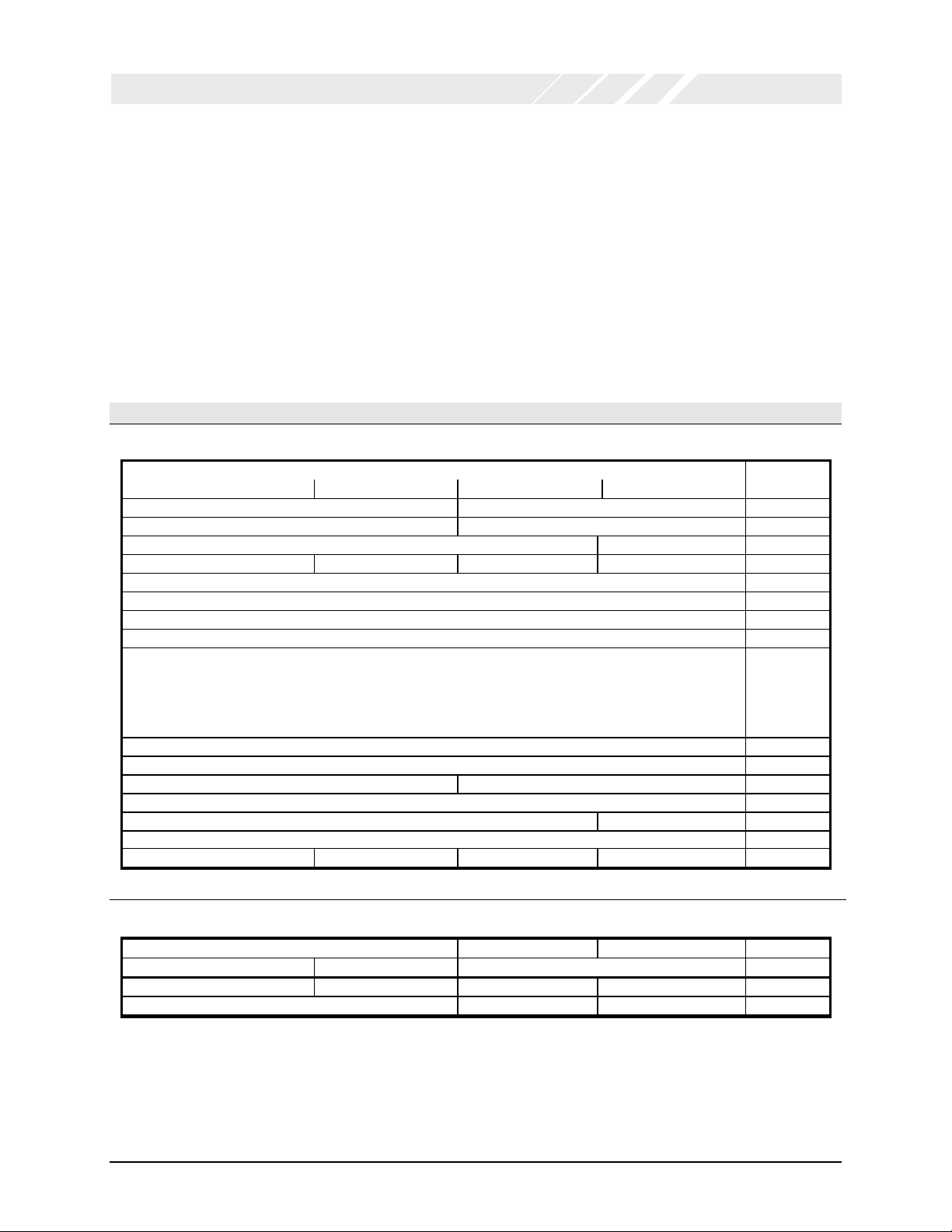
31 16 15 0
Device ID Vendor ID 00h
Status Command 04h
BIST1 Header Type Reserved Reserved 0Ch
Base Address Register 0 (BAR0) – UART Function in I/O space 10h
Base Address Register 1 (BAR 1) - UART Function in Memory space 14h
Base Address Register 2 (BAR 2) – Local Configuration Registers in IO space 18h
Base Address Register 3 (BAR3) – Local Configuration Registers in Memory space 1Ch
Base Address Register 4 (BAR4) – Cardbus Status Registers in Memory Space
Subsystem ID Subsystem Vendor ID 2Ch
Reserved Reserved Interrupt Pin Interrupt Line 3Ch
Configuration Register Description Offset
Class Code Revision ID 08h
Function Event : Offset +0
Function Event Mask : Offset +4
Function Present State : Offset +8
Function Force Event : Offset +12
Reserved (Bar 5) 24h
Cardbus CIS Pointer 28h
Reserved 30h
Reserved Cap_Ptr 34h
Reserved 38h
OXCB950
Address
20h
Predefined PCI Header Region
Device Dependant PCI Region
Power Management Capabilities (PMC) Next Ptr Cap_ID 40h
Reserved Reserved PMC Control/Status Register (PMCSR) 44h
Tuple Byte3* Tuple Byte 2* Tuple Byte1* Tuple Byte 0* 48h
… Tuple Byte (n+1)* Tuple Byte n* 4Ch
* Tuples are available for the Cardbus mode only. These fields return all 0’s for the PCI mode of the device.
Table 2: Cardbus/PCI Configuration space
Data Sheet Revision 1.1 Page 13

OXFORD SEMICONDUCTOR LTD.
Reset value Program read/write Register name
Cardbus Mode PCI Mode EEPROM PCI
Vendor ID 0x1415 1 W R
Device ID 0x950B 1 W R
Command 0x0000 - R/W
Status 0x0290 W(bit 4) R/W
Revision ID 0x00 1 - R
Class code 0x070006 1 W R
Header type 0x00 - R
BAR 0 0x00000001 - R/W
BAR 1 0x00000000 - R/W
BAR 2 0x00000001 - R/W
BAR 3 0x00000000 - R/W
BAR 4 0x00000000 - R/W
Cardbus CIS Pointer 0x00000048 (relocate3 = 0)
or
0x00000000
(no CIS)
W R
0x00000080 (relocate3 = 1)
Subsystem VID 0x1415 2 W R
Subsystem ID 0x0001 2 W R
Cap ptr. 0x40 - R
Interrupt line 0x00 1 - R/W
Interrupt pin 0x01 W R
Cap ID 0x01 - R
Next ptr. 0x00 - R
PM capabilities 0x6C01 W R
PMC control/ status
0x0000 - R/W
register
OXCB950
Table 3: Cardbus/PCI configuration space default values
1
For cardbus applications, the PC Card Standard 7.x defines these fields as “Allocated”. However, for cardbus support in
Windows, these fields need to be defined to fully support the PCI configuration Space.
2
For cardbus applications, the PC Card Standard 7.x defines these fields as “Reserved”. However, for cardbus support in
Windows, these fields need to be defined to fully support the PCI configuration Space.
3
Relocate is a bit in the local configuration registers that can locate the start of the cardbus information structure at DWORD18
or DWORD 32 in the PCI configuration region. This bit is writable only via the optional EEPROM. The default state is 0, so the
CIS is available at DWORD18 in the PCI configuration region.
Data Sheet Revision 1.1 Page 14

OXFORD SEMICONDUCTOR LTD.
OXCB950
6.3 Accessing the UART function
Access to the internal UART is achieved via standard I/O and memory mapping, at addresses defined by the Base Address
Registers (BARs) in the PCI configuration space. These BARs are configured by the system to allocate blocks of I/O and
memory space to this logical function, according to the size required by the function. The base addresses that have been
allocated can then be used to access this uart function. The mapping of these BARs is shown in the table below.
BAR UART Function
0 Internal UART (I/O Mapped)
1 Internal UART(Memory Mapped)
2 Local configuration registers (I/O Mapped)
3 Local configuration registers (Memory Mapped)
4 Cardbus Status Registers (Memory Mapped)
– relevant to cardbus mode only
5 Unused
Table 4: Base Address Register definition
6.3.1 Cardbus/PCI access to the internal UART
IO and memory space
BAR 0 and BAR 1 of function 0 are used to access the internal UART. The function reserves an 8-byte block of I/O space and a
4K byte block of memory space. Once the I/O and/or the Memory access enable bits in the Command register (of the PCI
configuration space) are set, the UART can be accessed following the mapping shown in Table 5.
UART
Address
(hex)
0 0
1 1
2 2
3 3
4 4
5 5
6 6
7 7
UART
Address
000 00
001 04
002 08
003 0C
004 10
005 14
006 18
007 1C
Cardbus/PCI Offset from Base Address 0
for Function0 in IO space (hex)
Cardbus/PCI Offset from Base Address 1
for Function0 in Memory space (hex)
Note 1: Since 4K of memory space is reserved and the full bus address is not used for decoding, there are a number of aliases of the UART in the allocated
memory region
Data Sheet Revision 1.1 Page 15
Table 5: Cardbus/PCI address map for the internal UART (I/O and memory)

OXFORD SEMICONDUCTOR LTD.
OXCB950
6.4 Accessing Local configuration registers
The local configuration registers are a set of device specific registers which can always be accessed, irrespective of the cardbus
or pci modes of the device. They are mapped to the I/O and memory addresses set up in BAR2 and BAR3, with the offsets
defined for each register. I/O or memory accesses can be byte, word or dword accesses, however on little-endian systems such
as Intel 80x86 the byte order will be reversed.
6.4.1 Local Configuration and Control register ‘LCC’ (Offset 0x00)
This register defines control of ancillary functions such as Power Management, endian selection and the serial EEPROM. The
individual bits are described below.
Bits Description Read/Write Reset
0 Cardbus Mode. This bit returns the state of the device.
1=> Cardbus Mode. 0 => PCI Mode.
1 Relocate Cardbus Information Structure.
0 => Make available CIS at DWORD18 in PCI configuration Space
1 => Make available CIS at DWORD32 in the PCI configuration Space
This bit has meaning only for cardbus applications.
2 Reserved - R 0
4:3 Endian Byte-Lane Select for memory access to UART function.
00 = Select Data[7:0] 10 = Select Data[23:16]
01 = Select Data[15:8] 11 = Select Data[31:24]
Memory access to UART registers is always DWORD aligned. When
accessing 8-bit regions this option selects the active byte lane. As both
cardbus/PCI and PC architectures are little endian, the default value will
be used by systems, however, some non-PC architectures may need to
select the byte lane.
7:5 Power-down filter time. These bits define a time value for an internal
filter that filters the device’s powerdown requests before the request is
recognised. Once Function0 is ready to go into the power down mode,
the OXCB950 will wait for the specified filter time and if Function0 is still
in the power-down request mode, it can assert a cardbus/PCI interrupt
000 = Power-down request disabled
001 = 4 seconds
10:8 Reserved: Power management test bits. The device driver must write
zero to these bits
20:11 Reserved. - R 000h
21 Source of Cardbus Information Structure. This bit returns which area
the tuple information had been provided.
0 => CIS from hardcoded Values
1 => CIS from RAM (Set when a download into the CIS zone was made)
This bit has meaning only for cardbus applications.
22 Enable Writes to Cardbus InformationStructure.
Provided that the CIS is contained in RAM (LCC[21]= ‘1’), then setting
this bit allows the tuple information contained in RAM to be written by
cardbus/pci configuration transactions. This does not update the CIS
information in the EEPROM.
This bit has meaning only for cardbus applications
010 = 129 seconds
011 = 518 seconds
1XX = Powerdown Immediate
EEPROM
W R 1
W R 0
W RW 00
W RW 000
- R 000
W R 0
W R/W 0
PCI
Data Sheet Revision 1.1 Page 16

OXFORD SEMICONDUCTOR LTD.
Bits Description Read/Write Reset
23 Enable Cardbus Status Registers
When set (1), all interrupt sources and power management events are
controlled by the INTR, GWAKE/WKUP fields of the cardbus status
registers.
This bit has meaning only for cardbus applications
24 EEPROM Clock. For reads or writes to the external EEPROM , toggle
this bit to generate an EEPROM clock (EE_CK pin).
25 EEPROM Chip Select. When 1 the EEPROM chip-select pin EE_CS is
activated (high). When 0 EE_CS is de-active (low).
26 EEPROM Data Out. For writes to the EEPROM, this output bit feeds the
input-data of the external EEPROM. This bit is output on the devices
EE_DO and clocked into the EEPROM by EE_CK.
27 EEPROM Data In. For reads from the EEPROM, this input bit is the
output-data (D0) of the external EEPROM connected to EE_DI pin.
28 EEPROM Valid.
A 1 indicates that a valid EEPROM program header is present
29 Reload configuration from EEPROM.
Writing a 1 to this bit re-loads the configuration from EEPROM. This bit is
self -clearing after an EEPROM read
30 Reserved - R 0
31 Reserved - R 0
EEPROM
W R/W 0
- RW 0
- RW 0
- RW 0
- R 1
- R X
- RW 0
OXCB950
PCI
6.4.2 Multi-purpose I/O Configuration register ‘MIC’ (Offset 0x04)
This register configures the operation of the multi-purpose I/O pins ‘MIO[1:0]’ as follows.
Bits Description Read/Write Reset
1:0 MIO0 Configuration Register
00 -> MIO0 is a non-inverting input pin
01 -> MIO0 is an inverting input pin
10 -> MIO0 is an output pin driving ‘0’
11 -> MIO0 is an output pin driving ‘1’
3:2 MIO1 Configuration Register
00 -> MIO1 is a non-inverting input pin
01 -> MIO1 is an inverting input pin
10 -> MIO1 is an output pin driving ‘0’
11 -> MIO1 is an output pin driving ‘1’
4 MIO0 Power Management Event Enable.
A value of ‘1’ enables the MIO0 pin to set the PME_Status bit in the PCI
PMCSR register, and hence assert the PME# (pci) or CSYSCHG
(cardbus) pin if this option has been enabled.
A value of ‘0’ prevents MIO0 from setting the PCI PME_Status bit.
5 MIO1 Power Management Event Enable.
A value of ‘1’ enables the MIO1 pin to set the PME_Status bit in the PCI
PMCSR register, and hence assert the PME# (pci) or CSYSCHG
(cardbus) pin if this option has been enabled.
A value of ‘0’ prevents MIO1 from setting the PCI PME_Status bit.
EEPROM
W RW 00
W RW 00
W RW 0
W RW 0
PCI
Data Sheet Revision 1.1 Page 17

OXFORD SEMICONDUCTOR LTD.
Bits Description Read/Write Reset
6 MIO0 Power Down Filter Control:
A ‘1’ enables the MIO0 pin to invoke a powerdown request via the power
down filter (if the filter is enabled). State of MIO0 that causes the
powerdown request is governed by the controls MIC[1:0).
7 MIO1 Power Down Filter Control:
A ‘1’ enables the MIO1 pin to invoke a powerdown request via the power
down filter (if the filter is enabled). State of MIO1 that causes the
powerdown request is governed by the controls MIC[3:2).
31:8 Reserved - R 00
EEPROM
W RW 0
W RW 0
OXCB950
PCI
6.4.3 UART Mirror Register ‘UMR’ (Offset 0x08):
The internal UART’s FIFO levels (both on the transmitter and receiver) and general interrupt source register, is mirrored
(shadowed) in the local configuration registers as follows
Bits Description Read/Write Reset
7:0 UART Receiver FIFO Level (RFL[7:0]) - R 00h
15:8 UART Transmitter FIFO Level (TFL[7:0]) - R 00h
21:16 UART Interrupt Source Register (ISR[5:0]) - R 01h
26:22 Reserved - R 00h
27 UART Good-Data Status - R 1h
31:28 Reserved - R 0h
Good-Data status for the internal UART is set when all of the following conditions are met:
• ISR reads a level0 (no-interrupt pending), a level 2a (receiver data available, a level 2b (receiver time-out) or a level 3
(transmitter THR empty) interrupt
• LSR[7] is clear so there is no parity error, framing error or break in the FIFO
• LSR[1] is clear so no over-run error has occurred
If the device driver software reads the receiver FIFO levels from this register, then if Good-Data status is set, the driver can
remove the number of bytes indicated by the FIFO level without the need to read the line status register. This feature enhances
the driver efficiency.
If the Good-Data status bit is not set, then the software driver should examine the ISR bits. If the ISR indicates a level 4 or higher
interrupt, the interrupt is due to a change in the state of modem lines or detection of flow control characters. The device driversoftware should then take appropriate measures as would in any other 550/950 driver. When ISR indicates a level 1 (receiver
status) interrupt then the driver can examine the Line Status Register (LSR) of the relevant channel. Since reading the LSR
clears LSR[7], the device driver-software should either flush or empty the contents of the receiver FIFO, otherwise the GoodData status will no longer be valid.
EEPROM
PCI
Data Sheet Revision 1.1 Page 18

OXFORD SEMICONDUCTOR LTD.
OXCB950
6.4.4 Global Interrupt Status and Control Register ‘GIS’ (Offset 0x0C)
This register controls the assertion of interrupts and power management events, as well as returning the internal status of all
interrupt sources and power management events.
Bits Description Read/Write Reset
1:0 Reserved - R 0x0h
2 MIO0 Internal State.
This bit reflects the state of the internal MIO[0] signal. The internal MIO[0]
signal reflects the non-inverted or inverted state of MIO0 pin. 2
3 MIO1 Internal State
This bit reflects the state of the internal MIO[1] signal. The internal MIO[1]
reflects the non-inverted or inverted state of MIO1 pin. 2
17-4 Reserved - R 0
18 MIO0 Interrupt Enable
When set (1) allows the pin MIO0 to assert an interrupt on the device’s INTA#
(CINT#) pin. The state of the MIO0 signal that causes an interrupt is
dependant upon the polarity set by the register fields MIC(1:0)
19 MIO1 Interrupt Enable
When set (1) allows the pin MIO1 to assert an interrupt on the device’s INTA#
(CINT#) pin. The state of the MIO1 signal that causes an interrupt is
dependant upon the polarity set by the register fields MIC(3:2)
20 Power-down Internal Interrupt Status.
This is a sticky bit. When set, it indicates that a power-down request has been
recognised (validated), which would normally have asserted a powerdown
interrupt on the INTA# (CINT#) pin if GIS bit 21 was set.
Reading this bit clears the Internal Powerdown Interrupt Status.
21 Power-down interrupt enable.
When set to ‘1’, a powerdown request is allowed to generate an interrupt on
the INTA#/ (CINT# ) pin.
22 UART interrupt status
. 1
This bit reflects the interrupt status of the internal UART.
23 UART Interrupt Enable.
When set (1) allows the UART to assert an interrupt on the device’s INTA#
(CINT# ) pin
3
24 UART Power Management Event Enable
A value of ‘1’ enables the UART ‘wakeup’ events to set the PME_Status bit in
the PCI PMCSR register, and hence assert the PME# (pci) or CSYSCHG
(cardbus) pin if this option has been enabled.
A value of ‘0’ prevents any wakeup events from the UART from setting the
PCI PME_Status bit.
25 UART Powerdown Filter Control
A ‘1’ enables the UART to invoke a powerdown request via the power down
filter (if the filter is enabled).
31:24 Reserved - R 00h
EEPROM
-
-
PCI
R
R
W RW 1
W RW 1
- R X
W RW 0
- R 0
W R/W 1
W R/W 0
W R/W 0
X
X
Data Sheet Revision 1.1 Page 19

OXFORD SEMICONDUCTOR LTD.
OXCB950
Note1 GIS(22) is the inverse of UMR(16).
Note 2: The returned value is either the direct state of the corresponding MIO pin or its inverse as configured by the Multi -purpose I/O Configuration register
Note 3: The UART Interrupt Enable register bit is set after a hardware reset to enable the interrupt from the internal UART. This will cater for generic device-
‘MIC’ (offset 0x04). As the internal MIO can assert a cardbus/PCI interrupt, the inversion feature can define each external interrupt to be defined as
active-low or active-high, as controlled by the MIC register.
driver software that does not access the Local Configuration Registers. The default setting for the UART Interrupt Enable bit can be changed using
the serial EEPROM. Note that even though by default the UART interrupt is enabled in this register, since after a reset the IER register of the UART
is disabled then a cardbus/PCI interrupt will not be asserted by the UART after a hardware reset.
6.5 Cardbus/ PCI Interrupt
Interrupts in cardbus/PCI systems are level-sensitive and
can be shared. In the OXCB950, there are three sources of
interrupts - two from the Multi-Purpose I/O pins (MIO0,
MIO1), and one from the internal UART.
Since the OXCB950 has only one interrupt pin (INTA# /
CINT#), the default routing information contained in the
device (the interrupt pin value) results in all interrupts being
made available on this single interrupt pin.
This default routing may be modified (to disable all
interrupts, for example) by writing to the Interrupt Pin field
in the cardbus/PCI configuration registers using the serial
EEPROM facility. The Interrupt Pin field is normally
considered a hard-wired read-only value in cardbus/PCI. It
indicates to system software which interrupt pin (if any) is
used by a function. The interrupt pin may only be modified
using the serial EEPROM facility, and card developers
must not set any value which violates the cardbus/PCI
specification on this issue. If in doubt, the default routings
should be used. Table 6 relates the Interrupt Pin field to the
device pin used.
Interrupt Pin Device Pin used
0 None
1 INTA# (CINT#)
2 to 255 Reserved
Table 6: ‘Interrupt pin’ definition
During the system initialisation process and cardbus/PCI
device configuration, system-specific software reads the
interrupt pin field to determine which (if any) interrupt pin is
used by the function. It programmes the system interrupt
router to logically connect this interrupt pin to a systemspecific interrupt vector (IRQ). It then writes this routing
information to the Interrupt Line field in the function’s
cardbus/PCI configuration space. Device driver software
must then hook the interrupt using the information in the
Interrupt Line field.
The Interrupt status for all sources of interrupts are
available using the GIS register in the Local Configuration
Register set, which can be accessed using I/O or Memory
accesses.
The 3 sources of interrupts on the OXCB950, can be
enabled/disabled individually using the options in the local
configuration register “GIS”.
By default, these options are enabled so that irrespective of
the device’s application mode (cardbus or pci) the
assertion of the 2 Multi_Purpose I/O pins (MIO0, MIO1)
will, following the initial cardbus/PCI configuration process,
assert the interrupt pin of the device. By the same token,
any UART based interrupts that are generated as a result
of enabling interrupts in the UART’s interrupt register (the
ISR register) will result in the assertion of the UART
interrupt on the interrupt pin of the device.
Once an interrupt has been asserted, this interrupt can only
be removed by the device driver either by disabling the
relevant controls in the GIS register or by removing the
conditions on the 3 interrupt sources. For the UART, this
will require reads of the relevant register to clear any UART
based interrupts.
Cardbus applications, normally expect a set of four 32-bit
registers: Function Event, Function Event Mask, Function
Present State, and Function Force Event Registers to
control the assertion/deassertion of interrupts (and power
management events). These are the cardbus status
registers located in memory space at the location given by
the CISTPL_CONFIG_CB tuple. For the OXCB950, these
registers reside at the memory base address register BAR4
that is dedicated to provide access to these additional
registers. By default, in cardbus mode, these status
registers are disabled (bypassed) so cardbus applications
exhibit the same interrupt behaviour as per the pci mode.
This default setting is particularly suitable for those
applications, such as Windows 9x, that treat cardbus
functions as PCI functions and continue to utilise (modified)
versions of PCI device drivers for cardbus functionality.
These PCI based device drivers do not expect the
presence of these cardbus status registers to further
control the interrupt generation / deassertion logic.
For those cardbus applications that do require use of these
cardbus status registers, these registers can be enabled by
setting LCC, bit 23 located in the device’s local
configuration registers. This can be achieved by performing
Data Sheet Revision 1.1 Page 20

OXFORD SEMICONDUCTOR LTD.
an I/O or Memory write to this bit in the local configuration
register or by using the optional EEPROM to download into
this area.
Once these cardbus status registers are enabled, interrupts
will only be asserted on the device’s interrupt pin provided
that the INTR field is enabled in the Function Event Mask
Register (disabled by default) and the corresponding INTR
field in the Function Event Register has detected (latched)
a valid internal interrupt request. Once asserted, the
interrupt on the device’s interrupt pin can only be disabled
by either disabling the INTR field in the Function Event
Mask register or by writing a “1” to the INTR field of the
6.6 Cardbus/PCI Power Management
OXCB950
Function Event Register. The INTR field in the Function
Present State register will reflect the current (non-latched)
state of any internal interrupt requests and the INTR field in
the Function Force register is available to generate
software based interrupts for debug purposes.
NOTE : Enabling of the cardbus status registers provides
additional controls to the interrupt generation/deassertion
logic. The interrupt controls in the local configuration
registers must nevertheless be enabled to detect the
interrupts from the device’s 3 interrupt sources in the first
place.
The OXCB950 is compliant with the Power Management
Requirements for cardbus PC cards as detailed in the
Electrical Specification of the PC Card Standard, release
7.x. It is also compliant to the PCI Power Management
Specification Revision 1.0. The device (function0)
implements a set of Power Management registers and
supports the power states D0, D2 and D3.
Power management is accomplished by handling the
power-down and power-up (“power management event”)
requests, that are asserted on the device’s interrupt pin
and the pins PME#/CSYSCHG respectively. Note, PME# is
the power management event for PCI applications and
CSYSCHG is the power management event for cardbus
applications. The logic behind these signals is identical.
Power-down requests are not defined by any of the Power
Management specifications. It is a device-specific feature
and requires a bespoke device driver implementation. The
device driver can either implement the power-down itself or
use a special interrupt and power-down features offered by
the device to determine when the device is ready for
power-down.
For PCI applications, it worth noting that the PME# pin can,
in certain cases, activate the PME# signal when power is
removed from the device, which will cause the PC to wake
up from Low-power state D3(cold). To ensure full crosscompatibility with system board implementations, use of an
isolator FET is recommended. If Power Management
capabilities are not required, the PME# pin can be treated
as no-connect. There are no such problems for cardbus
applications. The CSYSCHG line is not capable of being
asserted on removal of device power.
6.6.1 Power Management via UART/ MIO pins
Provided that the necessary controls have been set in the
device’s local configuration registers (LCC, MIC, and GIS),
the internal UART and the 2 multi_purpose (MIO) pins can
be programmed to issue powerdown requests and/or
‘wakeup’ requests (power management events).
For the case of the internal UART, the device can be
configured to monitor the activity of the serial channel, and
issue a power-down interrupt when the UART is inactive
(no interrupts pending and both transmitter and receiver
are idle).
For the case of the MIO pins, the MIO state that governs
powerdown is the inverse of the MIO state that asserts the
device’s interrupt pin (the INTA# / CINT# line, if that option
were to be enabled). This means that when any external
device is not interrupting it will automatically begin the
powerdown cycle.
When either a powerdown request from the internal UART
or a powerdown request from the MIO pins has been
detected, the internal power management circuitry waits for
a period of time as programmed into the Power-Down Filter
Time (defined by the local configuration register LCC[7:5])
and if the powerdown requests are still valid i.e. for the
UART, this means that the channel is still inactive, then the
OXCB950 can issue a powerdown interrupt on the device’s
interrupt pin if this option is enabled. Alternatively, the
device driver can poll the powerdown status field in the
local configuration register GIS[20] to determine a
powerdown request. This powerdown filter stops the
UART and the MIO pins from issuing too many powerdown
interrupts whenever the UART and MIO pin activity is
intermittent.
Data Sheet Revision 1.1 Page 21
 Loading...