

OXFORD OX9160-TQC33-A Datasheet

Oxford Semiconductor Ltd.
OX9160
PCI Peripheral Bridge with
EPP Parallel Port & 8/32 bit local bus
FEATURES
• 33MHz, 32-bit target PCI controller.
• Fully PCI 2.2 and PCI Power Management 1.0
compliant.
• 8- or 32-bit pass-through Local bus.
• IEEE1284 parallel port.
• Parallel port supports EPP mode for maximum data
transfer rate to printers, removable drives etc.
• Most operations complete within one PCI frame (no
retries).
• Supports shared interrupts
DESCRIPTION
The OX9160 is a low-cost, general purpose PCI bridge
solution designed to ease the migration to PCI of parallel
port cards and instrumentation devices. It is configurable to
provide either a Local bus interface or a bi-directional
parallel port.
Using the local bus function, legacy devices can be easily
accessed throught the target PCI interface, which is
compliant with version 2.2 of the PCI Bus Specification and
version 1.0 of PCI Power Management Specification. All
reads and writes are completed with a minimum of PCI wait
states, which ensures lower PCI bus occupancy than most
similar PCI bridge solutions.
The local bus can be configured to operate with either 8- or
32-bit data, using either Intel x86 style or Motorola style
signalling.
• 12 multi-purpose I/O pins which can be configured as
interrupt input pins.
• EEPROM interface for optional reconfiguration.
• Local bus operation via I/O or memory mapping.
• Local bus supports Intel or Motorola mode signalling.
• Existing driver support for common I/O solutions.
• On-chip oscillator.
• 5.0V operation.
• Low power CMOS.
• 160 TQFP package.
Alternatively the local bus can be disabled in favour of an
integrated IEEE 1284 EPP parallel port. The parallel port is
an IEEE 1284-compliant host interface, which supports
SPP, PS2 (bidirectional) and EPP modes.
The local Bus function is extremely flexible, allowing the
designer to customize the addressable space, divide it into
chip-select regions, access devices via I/O or memory
space mapping, and adjust the timings of all operations.
The default register values have been selected to support
many standard peripheral chips such as I/O controllers and
other ISA-type devices, however all such parameters can
be overwritten using an optional MicrowireTM serial
EEPROM.
69 Milton Park, Abingdon, Oxon, OX14 4RX, UK
Tel: +44 (0)1235 824900 Fax: +44(0)1235 821141
OX9160 Data Sheet Revision 1.1 – Feb. 1999
Oxford Semiconductor 1999
Part No. OX9160-TQC33-A

OX9160
OXFORD SEMICONDUCTOR LTD.
CONTENTS
1 BLOCK DIAGRAM ......................................................................................................................................3
2 PIN INFORMATION.....................................................................................................................................4
3 PIN DESCRIPTIONS...................................................................................................................................5
4 PCI TARGET CONTROLLER.....................................................................................................................8
4.1 OPERATION...............................................................................................................................................................8
4.2 CONFIGURATION SPACE.......................................................................................................................................... 8
4.2.1 PCI CONFIGURATION SPACE REGISTER MAP.....................................................................................................9
4.3 ACCESSING LOGICAL FUNCTIONS........................................................................................................................10
4.3.1 PCI ACCESS TO 8-BIT LOCAL BUS......................................................................................................................10
4.3.2 PCI ACCESS TO 32-BIT LOCAL BUS....................................................................................................................11
4.3.3 PCI ACCESS TO PARALLEL PORT......................................................................................................................11
4.4 ACCESSING LOCAL CONFIGURATION REGISTERS..............................................................................................12
4.4.1 LOCAL CONFIGURATION AND CONTROL REGISTER ‘LCC’ (OFFSET 0X00)..................................................... 12
4.4.2 MULTI-PURPOSE I/O CONFIGURATION REGISTER ‘MIC’ (OFFSET 0X04) .........................................................13
4.4.3 LOCAL BUS TIMING PARAMETER REGISTER 1 ‘LT1’ (OFFSET 0X08): ...............................................................14
4.4.4 LOCAL BUS TIMING PARAMETER REGISTER 2 ‘LT2’ (OFFSET 0X0C):.............................................................. 16
4.4.5 GLOBAL INTERRUPT STATUS AND CONTROL REGISTER ‘GIS’ (OFFSET 0X1C).............................................17
4.5 PCI INTERRUPTS.....................................................................................................................................................18
4.6 POWER MANAGEMENT........................................................................................................................................... 19
5 LOCAL BUS...............................................................................................................................................20
5.1 OVERVIEW...............................................................................................................................................................20
5.2 OPERATION.............................................................................................................................................................20
5.3 CONFIGURATION & PROGRAMMING......................................................................................................................21
5.4 CLOCK REFERENCES.............................................................................................................................................21
6 BIDIRECTIONAL PARALLEL PORT.......................................................................................................22
6.1 OPERATION AND MODE SELECTION.....................................................................................................................22
6.1.1 SPP MODE........................................................................................................................................................... 22
6.1.2 PS2 MODE............................................................................................................................................................22
6.1.3 EPP MODE........................................................................................................................................................... 22
6.1.4 ECP MODE (NOT SUPPORTED) ..........................................................................................................................22
6.2 PARALLEL PORT INTERRUPT ................................................................................................................................22
6.3 REGISTER DESCRIPTION........................................................................................................................................23
6.3.1 PARALLEL PORT DATA REGISTER ‘PDR’ ...........................................................................................................23
6.3.2 DEVICE STATUS REGISTER ‘DSR’......................................................................................................................23
6.3.3 DEVICE CONTROL REGISTER ‘DCR’...................................................................................................................24
6.3.4 EPP ADDRESS REGISTER ‘EPPA’.......................................................................................................................24
6.3.5 EPP DATA REGISTERS ‘EPPD1-4’.......................................................................................................................24
6.3.6 EXTENDED CONTROL REGISTER ‘ECR’.............................................................................................................24
7 SERIAL EEPROM......................................................................................................................................25
7.1 SPECIFICATION.......................................................................................................................................................25
7.2 EEPROM DATA ORGANISATION.............................................................................................................................25
7.2.1 ZONE0: HEADER ..................................................................................................................................................25
7.2.2 ZONE1: LOCAL CONFIGURATION REGISTERS...................................................................................................26
7.2.3 ZONE2: IDENTIFICATION REGISTERS................................................................................................................27
7.2.4 ZONE3: PCI CONFIGURATION REGISTERS........................................................................................................27
8 OPERATING CONDITIONS......................................................................................................................28
9 DC ELECTRICAL CHARACTERISTICS..................................................................................................28
Data Sheet Revision 1.1 Page 2
OX9160
OXFORD SEMICONDUCTOR LTD.
9.1 NON-PCI I/O BUFFERS.............................................................................................................................................28
9.2 PCI I/O BUFFERS.....................................................................................................................................................29
10 AC ELECTRICAL CHARACTERISTICS..............................................................................................30
10.1 PCI BUS....................................................................................................................................................................30
10.2 LOCAL BUS..............................................................................................................................................................30
11 TIMING WAVEFORMS..........................................................................................................................32
12 PACKAGE INFORMATION...................................................................................................................37
13 ORDERING INFORMATION.................................................................................................................37
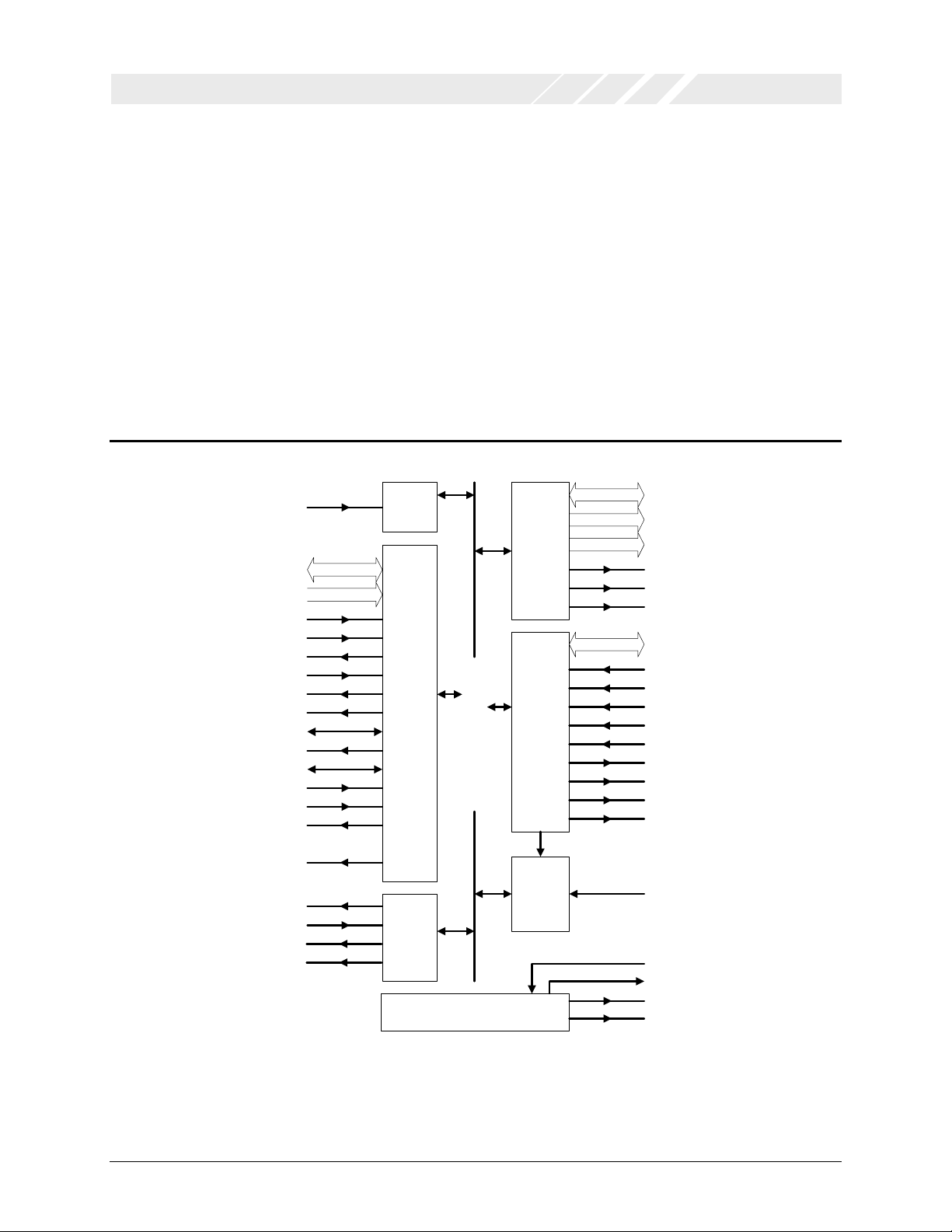
1 BLOCK DIAGRAM
MODE[1:0]
AD[31:0]
C/BE[3:0]#
CLK
FRAME#
DEVSEL#
IRDY#
TRDY#
STOP#
PAR
SERR#
PERR#
IDSEL
RST#
INTA#
Config.
interface
PCI
interface
Local Bus
Parallel
port
Internal Data / control bus
LBA[7:0]
LBD[7:0]
LBCS[3:0]
LBWR#
LBRD#
LBRST
PD[7:0]
ACK#
PE
BUSY
SLCT
ERR#
SLIN#
INIT#
AFD#
STB#
Data Sheet Revision 1.1 Page 3
PME#
EE_DO
EE_DI
EE_CS
Interrupt
logic
EEPROM
interfaceEE_CK
Crystal Oscillator
Figure 1 : OX9160 block diagram
MIO[11:0]
XTALI
XTALO
UART_Ck_Out
LBCLK

OX9160
OXFORD SEMICONDUCTOR LTD.
FRAME#
DEVSEL#
FRAME#
DEVSEL#
FRAME#
DEVSEL#
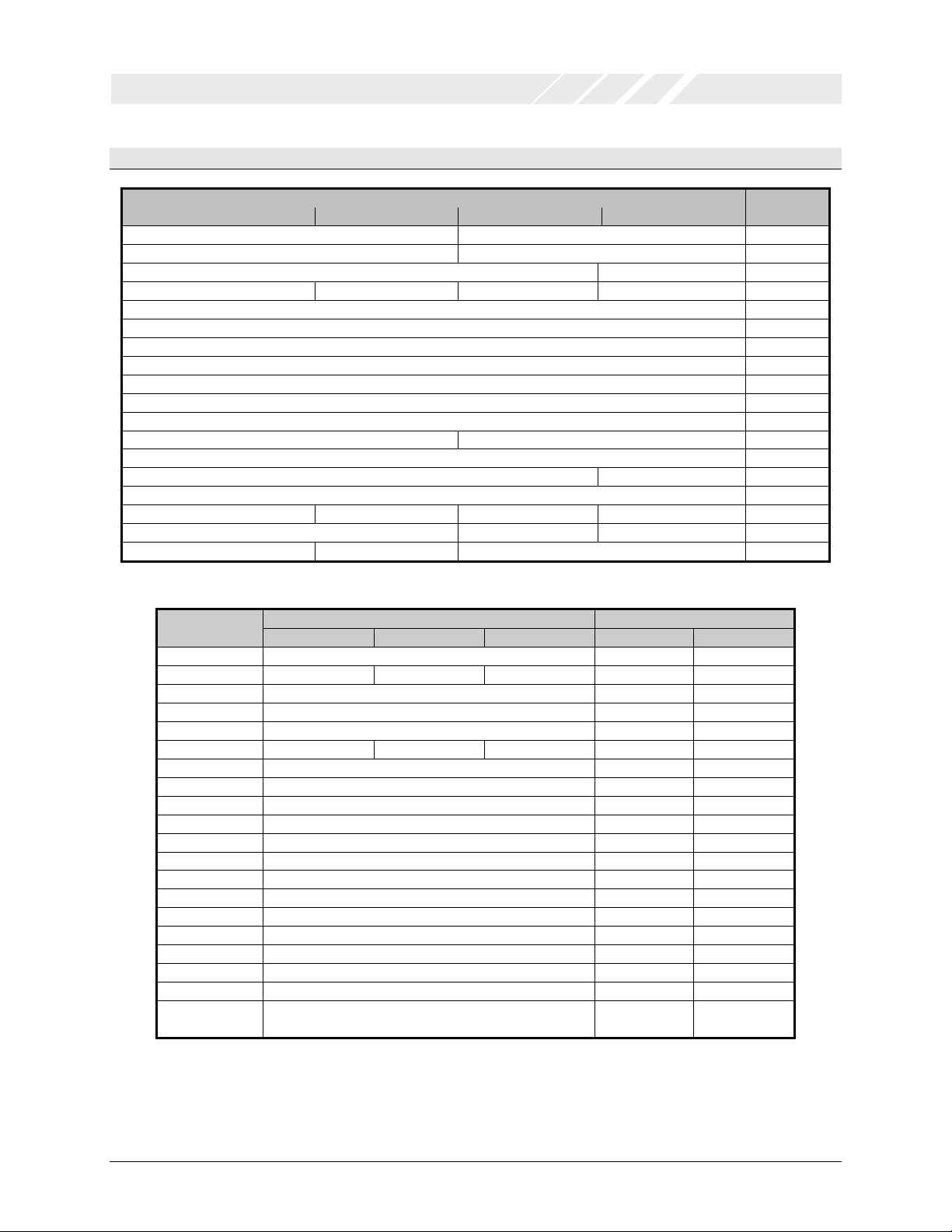
2 PIN INFORMATION
Mode ‘00’: 8-bit local bus
LBA1
LBA2
LBA3
LBCS0#
LBCS1#
LBCS2#
LBCS3#
LBRD#
LBWR#
VDD
GND
LBCLK
LBA4
LBA5
LBA6
LBA7
VDD
GND
120
119
118
117
116
115
114
113
112
111
110
109
108
107
106
105
104
PERR#
VDD
111
SERR#
GND
110
PAR
C/BE1#
LBCLK
LBA4
109
108
AD15
LBA5
107
AD14
LBA6
106
AD13
LBA7
105
103
18
VDD
GND
VDD
GND
104
103
18
LBA0
LBRST
LBRST#
MIO7
MIO6
MIO5
MIO4
MIO3
MIO2
MIO1
MIO0
INTA#
RST#
PME#
AD31
AD30
AD29
AD28
AD27
AD26
AD25
AD24
C/BE3#
IDSEL
AD23
AD22
AD21
AD20
AD19
AD18
LBA0
LBRST
LBRST#
MIO7
MIO6
MIO5
MIO4
MIO3
MIO2
MIO1
MIO0
INTA#
RST#
PME#
AD31
AD30
AD29
AD28
AD27
AD26
AD25
AD24
C/BE3#
IDSEL
AD23
AD22
AD21
AD20
AD19
AD18
121
122
123
124
125
126
127
128
129
130
131
132
NC
133
134
GND
135
CLK
136
VDD
137
138
139
140
141
GND
142
143
144
145
GND
146
VDD
147
148
149
150
151
152
GND
153
154
155
156
VDD
157
GND
158
159
160
OX9160-TQC33-A
1234567891011121314151617
GND
AD17
AD16
IRDY#
TRDY#
STOP#
C/BE2#
Mode ‘11’: 32-bit local bus
LBA1
LBA2
LBA3
LBCS0#
LBCS1#
LBCS2#
LBCS3#
LBRD#
LBWR#
120
119
118
117
116
115
114
113
121
122
123
124
125
126
127
128
129
130
131
132
NC
133
134
GND
135
CLK
136
VDD
137
138
139
140
141
GND
142
143
144
145
GND
146
VDD
147
148
149
150
151
152
GND
153
154
155
156
VDD
157
GND
158
159
160
112
OX9160-TQC33-A
1234567891011121314151617
LBDOUT
LBD0
LBD1
LBD2
LBD3
VDD
GND
LBD4
LBD5
LBD6
LBD7
MIO8
MIO9
MIO10
MIO11
99989796959493929190898887
102
101
100
1920212223242526272829303132333435
AD9
AD8
AD7
AD6
AD5
VDD
GND
AD12
AD11
AD10
LBDOUT
LBD0
LBD1
LBD2
LBD3
VDD
99989796959493929190898887
102
101
100
1920212223242526272829303132333435
AD4
VDD
GND
GND
C/BE0#
GND
LBD4
LBD5
LBD6
LBD7
MIO8
MIO9
MIO10
MIO11
GND
AD3
LBD8
GND
GND
GND
8584838281
86
3637383940
AD2
AD1
GND
LBD9
LBD10
LBD11
8584838281
86
3637383940
GNDNCNC
AD0
EE_CS
LBD12
LBD13
EE_DO
LBD14
80
NC
79
NC
78
NC
77
NC
76
GND
75
GND
74
GND
73
GND
72
VDD
71
XTL_Ck_Out
70
GND
69
GND
68
GND
67
GND
66
GND
65
VDD
64
XTLO
63
XTLI
62
GND
61
GND
60
GND
59
NC
58
NC
57
VDD
56
GND
55
NC
54
NC
53
NC
52
NC
51
GND
50
GND
49
GND
48
GND
47
GND
46
GND
45
Mode0
44
Mode1
43
NC
42
EE_DI
41
EE_CK
80
LBD15
79
LBA8
78
LBA9
77
LBA10
76
LBA11
75
NC
74
NC
73
NC
72
VDD
71
XTL_Ck_Out
70
GND
69
NC
68
LBD16
67
LBD17
66
LBD18
65
VDD
64
XTLO
63
XTLI
62
GND
61
LBD19
60
LBD20
59
LBD21
58
LBD22
57
VDD
56
GND
55
LBD23
54
LBD24
53
LBD25
52
LBD26
51
LBD27
50
LBD28
49
LBD29
48
LBD30
47
LBD31
46
GND
45
Mode0
44
Mode1
43
NC
42
EE_DI
41
EE_CK
PE
121
ACK#
122
NC
123
MIO7
124
MIO6
125
MIO5
126
MIO4
127
MIO3
128
MIO2
129
MIO1
130
NC
131
INTA#
RST#
PME#
AD31
AD30
AD29
AD28
AD27
AD26
AD25
AD24
C/BE3#
IDSEL
AD23
AD22
AD21
AD20
AD19
AD18
132
NC
133
134
GND
135
CLK
136
VDD
137
138
139
140
141
GND
142
143
144
145
GND
146
VDD
147
148
149
150
151
152
GND
153
154
155
156
VDD
157
GND
158
159
160
Mode ‘01’: Parallel port
BUSY
SLCT
ERR#NCNCNCNCNCNC
VDD
GNDNCSLIN#
INIT#
AFD#
STB#
VDD
NC
PD0
PD1
PD2
PD3
GND
120
119
118
117
116
115
114
113
112
111
110
109
108
107
106
105
99989796959493929190898887
104
102
101
100
103
OX9160-TQC33-A
1234567891011121314151617
GND
AD17
AD16
IRDY#
TRDY#
STOP#
PERR#
C/BE2#
SERR#
PAR
C/BE1#
AD15
AD14
AD13
GND
1920212223242526272829303132333435
18
VDD
VDD
GND
AD12
AD11
AD10
GND
GND
GNDNCNC
VDD
GND
PD4
PD5
PD6
AD9
AD8
AD7
GND
C/BE0#
GND
PD7
MIO8
MIO9
MIO10
MIO11
GND
8584838281
86
80
NC
79
NC
78
NC
77
NC
76
GND
75
GND
74
GND
73
GND
72
VDD
71
NC
70
GND
69
GND
68
GND
67
GND
66
GND
65
VDD
64
NC
63
NC
62
GND
61
GND
60
GND
59
NC
58
NC
57
VDD
56
GND
55
NC
54
NC
53
NC
52
NC
51
GND
50
GND
49
GND
48
GND
47
GND
46
GND
45
Mode0
44
Mode1
43
NC
42
EE_DI
41
3637383940
AD2
AD1
AD6
AD5
AD4
AD3
VDD
GND
GND
EE_CK
AD0
EE_CS
EE_DO
GND
AD17
AD16
IRDY#
TRDY#
C/BE2#
Data Sheet Revision 1.1 Page 4
STOP#
PERR#
SERR#
AD2
AD1
PAR
C/BE1#
AD15
AD14
AD13
AD9
AD8
AD7
AD6
VDD
VDD
GND
GND
GND
AD12
AD11
AD10
C/BE0#
AD0
AD5
AD4
AD3
VDD
GND
GND
EE_CS
EE_DO
Figure 2: Pinout in all configurable modes (package = 160 TQFP)

OX9160
OXFORD SEMICONDUCTOR LTD.
3 PIN DESCRIPTIONS
Mode
Dir Name Description
00 01 11
PCI Interface
139, 140, 141, 143, 144, 145,
148, 149, 152, 154, 155, 156,
159, 160, 1, 2, 14, 15, 16, 19,
20, 23, 24, 26, 28, 29, 32, 33,
34, 36, 37, 38
P_I/O AD[31:0] Multiplexed PCI Address/Data bus
150, 3, 13, 27 P_I C/BE[3:0]# PCI Command/Byte enable
136 P_I CLK PCI system clock
4 P_I FRAME# Cycle Frame
7 P_O DEVSEL# Device Select
5 P_I IRDY# Initiator ready
6 P_O TRDY# Target ready
9 P_O STOP# Target Stop request
12 P_I/O PAR Parity
11 P_O SERR# System error
10 P_I/O PERR# Parity error
151 P_I IDSEL Initialization device select
134 P_I RST# PCI system reset
132 P_OD INTA # PCI interrupt
138 P_OD PME# Power management event
Local bus
122 N/A 122 O LBRST Local bus active-high reset
123 N/A 123 O LBRST# Local bus active-low reset
102 O LBDOUT Local bus data out enable. This pin can be used by external
transceivers; it is high when LBD[7:0] are in output mode and low
when they are in input mode.
114-7 N/A 114-7 O
112 N/A 112 O
113 N/A 113 O
105-8
118-21
N/A
92-5
98-101
N/A
N/A
N/A
N/A
N/A
N/A
76-9,
105-8,
118-21
N/A
47-55,
58-61,
66-68,
80-87,
92-95,
98-101
I/O
I/O
O
O
Z
O
O
LBCS[3:0]#
LBDS[3:0]#
LBWR#
LBRDWR#
LBRD#
Hi-Z
LBA[7:0]
LBA[12:0]
LBD[7:0]
LBD[31:0]
Local bus active-low Chip-Select (Intel mode)
Local bus active-low Data-Strobe (Motorola mode)
Local bus active-low write-strobe (Intel mode)
Local bus Read-not-Write control (Motorola mode)
Local bus active-low read-strobe (Intel mode)
Permanent high impedance (Motorola mode)
(8-bit mode) Local bus address signals
(32-bit mode) Local bus address signals
(8-bit mode) Local bus data signals
(32-bit mode) Local bus data signals
Data Sheet Revision 1.1 Page 5

OX9160
OXFORD SEMICONDUCTOR LTD.
Parallel port
N/A 122 N/A I
N/A 121 N/A I PE Paper Empty. Activated by printer when it runs out of paper.
N/A 120 N/A I
N/A 108 N/A OD SLIN# Select (SPP mode). Asserted by host to select the peripheral
N/A 119 N/A I SLCT Peripheral selected. Asserted by peripheral when selected.
N/A 118 N/A I ERR# Error. Held low by the peripheral during an error condition.
N/A 107 N/A OD INIT# Initialize (SPP mode). Commands the peripheral to initialize.
N/A 106 N/A OD AFD# Auto Feed (SPP mode, open-drain)
N/A 105 N/A OD STB# Strobe (SPP mode). Used by peripheral to latch data currently
N/A Bus N/A I/O PD[7:0] Parallel data bus
EEPROM pins
41 O EE_CK EEPROM clock
39 O EE_CS EEPROM active-high Chip Select
42 IU EE_DI EEPROM data in. When the serial EEPROM is connected, this pin
40 O EE_DO EEPROM data out.
Miscellaneous pins
63 I XTLI Crystal oscillator input
64 O XTLO Crystal oscillator output. Maximum frequency 60MHz
71 O XTL_Ck_Out Buffered crystal clock output. This clock can drive TTL clock
109 O LBCLK Buffered PCI clock. Can be enabled/disabled by software
44,45 I Mode[1:0] Mode selector:
Power & Ground
18, 31, 57, 72, 97, 111,
147, 157
22, 65, 104, 137 V DC VDD Power supply. Supplies power to core logic, input buffers and
8, 17, 25, 30, 35, 56, 70,
96, 110, 142, 146, 153,
158
21, 46, 47, 48, 49, 50, 51,
60, 61, 62, 66, 67, 68, 69,
73, 74, 75, 76, 83, 84, 85,
86, 87, 103, 135,
ACK#
BUSY
V AC VDD Supplies power to output buffers in switching (AC) state
G AC GND Supplies GND to output buffers in switching (AC) state
G DC GND Ground (0 volts). Supplies GND to core logic, input buffers and
Acknowledge (SPP mode). ACK# is asserted (low) by the
peripheral to indicate that a successful data transfer has taken
place.
Busy (SPP mode). BUSY is asserted (high) by the peripheral when
it is not ready to accept data
available on PD[7:0]
should be pulled up using 1-10k resistor. When the EEPROM is
not used the internal pullup is sufficient.
signals from a clock generator circuit connected at XTLI & XTLO.
Can be enabled/disabled by software.
00: 8-bit local bus
01: Parallel port
11: 32-bit local bus
output buffers in steady state
output buffers in steady state
Data Sheet Revision 1.1 Page 6
Table 1: Pin Descriptions

OX9160
OXFORD SEMICONDUCTOR LTD.
Multi-purpose & External interrupt pins
131
N/A
N/A
131
131
N/A
I/O
Z
MIO0
Hi-Z
Multi-purpose I/O 0. Can drive high or low, or assert a PCI
interrupt
Permanent high impedance
130 I/O MIO1 Multi-purpose I/O 1. Can drive high or low, or assert a PCI
interrupt.
124-128
88-91
129 I/O
124-128
88-91
124-128
88-91
I
I/O MIO[11:3] Multi-purpose I/O pins. Can drive high or low, or assert a PCI
MIO2
PME_In
Multi-purpose I/O 2. When LCC[7] = 0, this pin can drive high or
low, or assert a PCI interrupt.
Input power management event. When LCC[7] is set this input pin
can assert a function1 PME#
interrupt
Note 1: Direction key:
I Input
IU Input with internal pull-up
O Output
I/O Bi-directional
OD Open drain
NC No connect
Z High impedance
P_I PCI input
P_O PCI output
P_I/O PCI bi-directional
P_OD PCI open drain
G Ground
V 5.0V power
Note 2: Power & Ground
There are two GND and two VDD rails inside the device. One set of rails supply power and ground to output buffers while in
switching state (called AC power) and another rail supply the core logic, input buffers and output buffers in steady-state (called
DC rail). The rails are not connected internally. This precaution reduces the effects of simultaneous switching outputs and
undesirable RF radiation from the chip. Further precaution is taken by segmenting the GND and VDD AC rails to isolate the PCI,
Local bus and parallel port pins.
Also, some GND pins (italicised) serve as GND in mode ‘00’ and mode ‘01’; however they are multiplexed and function as
address/data pins in mode ‘11’.
Data Sheet Revision 1.1 Page 7

OX9160
OXFORD SEMICONDUCTOR LTD.
4 PCI TARGET CONTROLLER
4.1 Operation
The OX9160 responds to the following PCI transactions:-
• Configuration access: The OX9160 responds to type 0
configuration reads and writes if the IDSEL signal is
asserted and the bus address is selecting a valid
configuration register. The device will respond to the
configuration transaction by asserting DEVSEL#. Data
transfer then follows. Any other configuration
transaction will be ignored by the OX9160.
• IO reads/writes: The address is compared with the
addresses reserved in the I/O Base Address Registers
(BARs). If the address falls within one of the assigned
ranges, the device will respond to the IO transaction
by asserting DEVSEL#. Data transfer follows this
address phase. For the parallel port and 8-bit Local
bus functions, only byte accesses are supported;
however the 32-bit bridge function also supports word
and dword accesses. For IO accesses to these
regions, the controller compares AD[1:0] with the byteenable signals as defined in the PCI specification. The
access is always completed; however if the correct BE
signal is not present the transaction will have no effect
• Memory reads/writes: These are treated in the same
way as I/O transactions, except that the memory
ranges are used. Memory access to single-byte
regions is always expanded to DWORDs in the
OX9160. In other words, OX9160 reserves a DWORD
per byte in single-byte regions. The device allows the
user to define the active byte lane using LCC[4:3] so
that in Big-Endian systems the hardware can swap the
byte lane automatically. For Memory mapped access
in single-byte regions, the OX9160 compares the
asserted byte-enable with the selected byte-lane in
LCC[4:3] and completes the operation if a match
occurs, otherwise the access will complete normally
on the PCI bus, but it will have no effect on the actual
controller.
• All other cycles (64-bit, special cycles, reserved
encoding etc.) are ignored.
The OX9160 will complete all transactions as disconnectwith-data, ie the device will assert the STOP# signal
alongside TRDY#, to ensure that the Bus Master does not
continue with a burst access. The exception to this is Retry,
which will be signalled in response to any access while the
OX9160 is reading from the serial EEPROM.
The OX9160 performs medium-speed address decoding as
defined by the PCI specification. It asserts the DEVSEL#
bus signal two clocks after FRAME# is first sampled low on
all bus transaction frames which address the chip. Fast
back-to-back transactions are supported by the OX9160 as
a target, so a bus master can perform faster sequences of
write transactions to the Local bus when an inter-frame
turn-around cycle is not required.
The device supports any combination of byte-enables to
the PCI Configuration Registers, the Local Configuration
registers (see Base Address 2 and 3) and the Local bus
controller in 32-bit mode. If a byte-enable is not asserted,
that byte is unaffected by a write operation and undefined
data is returned upon a read.
The OX9160 performs parity generation and checking on
all PCI bus transactions as defined by the standard. If a
parity error occurs during the PCI bus address phase, the
device will report the error in the standard way by asserting
the SERR# bus signal. However if that address/command
combination is decoded as a valid access, it will still
complete the transaction as though the parity check was
correct.
4.2 Configuration space
All required fields in the standard configuration space
header are implemented, plus the Power Management
Extended Capability register set. The format of the
configuration space is shown in Table 2 overleaf.
In general, writes to any registers that are not implemented
are ignored, and all reads from unimplemented registers
return 0.
Data Sheet Revision 1.1 Page 8
OX9160
OXFORD SEMICONDUCTOR LTD.
4.2.1 PCI Configuration Space Register map
Configuration Register Description Offset
31 16 15 0
Device ID Vendor ID 00h
Status Command 04h
Class Code Revision ID 08h
BIST1 Header Type Reserved Reserved 0Ch
Base Address Register 0 (BAR0) 10h
Base Address Register 1 (BAR 1) 14h
Base Address Register 2 (BAR 2) – Local Configuration Registers in IO space 18h
Base Address Register 3 (BAR3) – Local Configuration Registers in Memory space 1Ch
Reserved 20h
Reserved 24h
Reserved 28h
Subsystem ID Subsystem Vendor ID 2Ch
Reserved 30h
Reserved Cap_Ptr 34h
Reserved 38h
Reserved Reserved Interrupt Pin Interrupt Line 3Ch
Power Management Capabilities (PMC) Next Ptr Cap_ID 40h
Reserved Reserved PMC Control/Status Register (PMCSR) 44h
Address
Table 2: PCI Configuration space
Reset value Program read/write Register name
8-bit local bus 32-bit local bus Parallel port EEPROM PCI
Vendor ID 0x1415 W R
Device ID 0x9511 0x9512 0x9513 W R
Command 0x0000 - R/W
Status 0x0290 W (bit 4) R/W
Revision ID 0x00 - R
Class code 0x068000 0x068000 0x070101 W R
Header type 0x80 - R
BAR 0 0x00000001 - R/W
BAR 1 0x00000000 - R/W
BAR 2 0x00000001 - R/W
BAR 3 0x00000000 - R/W
Subsystem VID 0x1415 W R
Subsystem ID 0x0000 W R
Cap ptr. 0x40 - R
Interrupt line 0x00 - R/W
Interrupt pin 0x01 - R
Cap ID 0x01 - R
Next ptr. 0x00 - R
PM capabilities 0x6C01 W R
PMC control/
status register
0x0000 - R/W
Data Sheet Revision 1.1 Page 9
Table 3: PCI configuration space default values
OX9160
OXFORD SEMICONDUCTOR LTD.
4.3 Accessing logical functions
Access to the local bus and parallel port is achieved via standard I/O and memory mapping, at addresses defined by the Base
Address Registers (BARs) in configuration space. The BARs are configured by the system to allocate blocks of I/O and memory
space to the logical functions, according to which function is enabled and the size required. The addresses allocated can then be
used to access the functions. The mapping of these BARs is shown in Table 4.
BAR Local bus Parallel port
0 Local bus (I/O mapped) Parallel port base registers (I/O mapped)
1 Local bus (memory mapped) Parallel port extended registers (I/O mapped)
2 Local configuration registers (I/O mapped)
3 Local configuration registers (memory mapped)
4 Unused
5 Unused
Table 4: Base Address Register definition
4.3.1 PCI access to 8-bit local bus
BAR 0 and BAR 1 are used to access the Local bus. The
system allocates a block of I/O space and a block of
memory space according to the size requested.
I/O space
In order to minimise the usage of IO space, the block size
for BAR0 (I/O access) is user definable in the range of 4 to
256 bytes. Having assigned the address range, the user
can define two adjacent address bits to decode up to four
chip selects internally. This facility allows glueless
implementation of the local bus connecting to four external
peripheral chips. The address range and the lower address
bit for chip-select decoding (Lower-Address-CS-Decode)
are defined in the Local bus Configuration register (see
LT2[26:20] in section 1.1).
The 8-bit Local bus has eight address lines (LBA[7:0])
which correspond to the maximum IO address space. If the
maximum allowable block size is allocated to the IO space
(i.e. 256 bytes), then as access in IO space is byte aligned,
LBA[7:0] equal PCI AD[7:0] respectively. When the user
selects an address range which is less than 256 bytes, the
unused upper address lines will be set to logic zero.
The region can be divided into four chip-select regions
when the user selects the second uppermost non-zero
address bit for chip-select decoding. For example if 32bytes of IO space are reserved, the local bus address lines
A[4:0] are active and the remaining address lines are set to
zero. To generate four chip-selects the user should select
A3 as the Lower-Address-CS-Decode. In this case A[4:3]
will be used internally to decode chip-selects, asserting
LBCS0# when the address offset is 00-07h, LBCS1# when
offset is 08-0Fh, LBCS2# when offset is 10-17h, and
LBCS3# when offset is 18- 1Fh.
The region can be divided into two chip-select regions by
selecting the uppermost address bit to decode chip selects.
In the above example, the user can select A4 as the
Lower-Address-CS-Decode, thus using A[5:4] internally to
decode chip selects. As in this example LBA5 is always
zero, only chip-select lines LBCS0# and LBCS1# will be
decoded into, asserting LBCS0# when address offset is 000Fh and LBCS1# when offset is 10-1Fh.
The region can be allocated to a single chip-select region
by assigning an address bit beyond the selected range to
Lower-Address-CS-Decode (but not above A8). In the
above example, if the user selects A5 as the LowerAddress-CS-Decode, A[6:5] will be used to internally
decode chip-selects. As in this example LBA[7:5] are
always zero, only the chip select line LBCS0# may be
selected. In this case address offset 00-1Fh asserts
LBCS0# and the other chip-select lines remain inactive
permanently.
Memory Space:
The memory base address registers have an allocated
fixed size of 4K bytes in the address space. Since the
Local bus has 8 address lines and the OX9160 only
implements DWORD aligned accesses in memory space,
the 256 bytes of addressable space per chip select is
expanded to 1K. Unlike an I/O access, for a memory
access the unused upper address lines are always active
and the internal chip-select decoding logic ignores the user
setting for Lower-Address-CS-Decode (LT2[26:23]) and
uses PCI AD[11:10] to decode into 4 chip-select regions.
When the Local bus is accessed in memory space, A[9:2]
are asserted on LBA[7:0]. The chip-select regions are
defined in Table 5.
Data Sheet Revision 1.1 Page 10

OX9160
OXFORD SEMICONDUCTOR LTD.
Local bus
Chip-Select
(Data-Strobe)
LBCS0# (LBDS0#) 000h 3FCh
LBCS1# (LBDS1#) 400h 7FCh
LBCS2# (LBDS2#) 800h BFCh
LBCS3# (LBDS3#) C00h FFCh
Table 5: PCI address map for local bus (memory)
Note: The description given for I/O and memory accesses
is for an Intel-type configuration for the Local bus. For
Motorola-type configuration, the chip select pins are
redefined to data strobe pins. In this mode the Local bus
offers up to 8 address lines and four data-strobe pins.
PCI Offset from BAR 1
(Memory space)
Lower Address Upper Limit
4.3.2 PCI access to 32-bit local bus
Access to the Local bus in 32-bit mode is similar to 8-bit
mode (see section 4.3.1) with the following exceptions:
• The local Bus offers a 32-bit bi-directional data bus
and 12 bit address bus
• The PCI address signals ‘AD[13:2]’ are asserted on
LBA[11:0]
• Block size in memory space is programmable by
LT2[28:27] (see section 1.1)
• The Lower-Address-CS-Decode (LT2[26:23])
parameter is used to decode up to 4 chip selects
The block size allocation for chip-select regions is defined
in Table 6.
Number
of Chip
selects
1 16 ‘01’ ‘1010’
2 16 ‘01’ ‘1001’
4 16 ‘01’ ‘1000’
1 4 ‘00’ ‘1000’
2 4 ‘00’ ‘0111’
4 4 ‘00’ ‘0110’
Table 6: PCI access to 32-bit local bus (memory)
Memory
block size
(Kbytes)
LT2[28:27] LT2[26:23]
4.3.3 PCI access to parallel port
When the parallel port is enabled (Mode 01), access to the
port works via BAR definitions as usual, except that there
are two I/O BARs corresponding to two sets of registers
defined to operate a bi-directional Parallel Port. Memory
mapped access to the parallel port is not supported.
The user can change the I/O space block size of BAR0 by
over-writing the default values in LT2[25:20] using the
serial EEPROM (see section 1.1). For example the user
can reduce the allocated space for BAR0 to 4-bytes by
setting LT2[22:20] to ‘001’. The I/O block size allocated to
BAR1 is fixed at 8-Bytes.
Legacy PC parallel ports expect the upper register set to
be mapped 0x400 above the base block, therefore if the
BARs are fixed with this relationship, generic parallel port
drivers can be used to operate the device in all modes.
Example: BAR0 = 0x00000379 (8 bytes at address 0x378)
BAR1 = 0x00000779 (8 bytes at address 0x778)
If this relationship is not used, custom drivers will be
needed.
Data Sheet Revision 1.1 Page 11

OX9160
OXFORD SEMICONDUCTOR LTD.
4.4 Accessing Local configuration registers
The local configuration registers are a set of device specific registers which are used to configure the controller. They are
mapped to the I/O and memory addresses set up in BAR2 and BAR3, with the offsets defined for each register. Access is limited
to byte only for I/O accesses; memory accesses can also be word or dword accessed, however on little-endian systems such as
Intel 80x86 the byte order will be reversed.
4.4.1 Local Configuration and Control register ‘LCC’ (Offset 0x00)
This register defines control of ancillary functions such as Power Management, external clock reference signals and the serial
EEPROM. The individual bits are described below.
Bits Description Read/Write Reset
1:0 Mode. These bits return the state of the Mode[1:0] pins. - R XX
2 Enable crystal clock output. When this bit is set, the crystal oscillator
output pin (XTL_Ck_Out) is active. When low, XTL_Ck_Out is
permanently low.
4:3 Endian Byte-Lane Select for memory access to 8-bit Local bus.
00 = Select Data[7:0] 10 = Select Data[23:16]
01 = Select Data[15:8] 11 = Select Data[31:24]
Memory access to OX9160 is always DWORD aligned. When accessing
8-bit regions like the 8-bit Local bus and the parallel port, this option
selects the active byte lane. As both PCI and PC architectures are little
endian, the default value will be used by systems, however, some nonPC architectures may need to select the byte lane. These bits are
ignored in 32-bit Local bus.
6:5 Reserved. These bits are used for test purposes. The device driver must
write zeros to these bits.
7 MIO2_PME Enable. A value of ‘1’ enables the MIO2 pin to set the
PME_Status in PMCSR register, and hence assert the PME# pin if
enabled. A value of ‘0’ disables MIO2 from setting the PME_Status bit
(see section 4.6).
23:8 Reserved. These bits are used for test purposes. The device driver must
write zeros to these bits.
24 EEPROM Clock. For PCI read or write to the EEPROM , toggle this bit to
generate an EEPROM clock (EE_CK pin).
25 EEPROM Chip Select. When 1 the EEPROM chip-select pin EE_CS is
activated (high). When 0 EE_CS is de-active (low).
26 EEPROM Data Out. For writes to the EEPROM, this output bit is the
input-data of the EEPROM. This bit is output on EE_DO and clocked into
the EEPROM by EE_CK.
27 EEPROM Data In. For reads from the EEPROM, this input bit is the
output-data of the EEPROM connected to EE_DI pin.
28 EEPROM Valid. A 1 indicates that a valid EEPROM program is present - R X
29 Reload configuration from EEPROM. Writing a 1 to this bit re-loads the
configuration from EEPROM. This bit is self-clearing after EEPROM read
30 Reserved - - 0
31 Reserved - R 0
EEPROM
W RW 0
W RW 00
- R 00
W RW 0
- R 0000h
- RW 0
- RW 0
- RW 0
- R X
- RW 0
PCI
Data Sheet Revision 1.1 Page 12
 Loading...