

OXFORD OX16PCI958 DATA SHEET

EATURES
F
OX16PCI958 DATA SHEET
Octal UART
with PCI Interface
• Efficient 32-bit, 33
PCI controller, compliant to PCI Local Bus
Specification 3.0 & PCI Power Management
Specification 1.1
• Eight UARTs fully software compatible with 16C550-
type devices
• Compatible with existing 16C550/450 device drivers
• PCI 2.1, 2.2, 2.3 & 3.0 compliant
• Supports both 5.0-V & 3.3-V PCI signalling
• 32-byte deep FIFO per transmitter & receiver
• Baud rates up to 4.125 Mega-baud (using a
16.5 MHz input clock).
• Clock can be provided from crystal oscillator or
external clock source
• Automated out-of-band flow control using
CTS#/RTS#
• Configuration data is held in a small, low-cost serial
Microwire
TM
1
/3 MHz multi-function, target-only
compatible EEPROM
DESCRIPTION
The OX16PCI958 contains eight UARTs (Universal
Asynchronous Receiver-Transmitters) and a host
interface suitable for direct connection to a PCI bus.
Once installed and configured by the host OS, it provides
an eight-byte programming interface to each UART. The
UARTs are fully software-compatible with 16C550
devices. The device can be configured to fit the
requirements of RS232 or RS422 applications.
The UARTs convert between RS232-format serial data
on separate transmit and receive lines, and byte-wide I/O
writes and reads on the host interface. Malformed
incoming serial data is flagged along with the data in the
receive FIFO. The state of the UART can be found at
any time by reading status registers, and modem control
(handshaking output) lines can be individually controlled.
Although polled-mode operation is possible, the UART
will usually be operated on a host-interrupt basis. The
interrupt system is designed to allow efficient handling of
• Driver-facilitated DSR/DTR & Xon/Xoff handshaking
• 5-,6-,7- & 8-bit data framing
• 1, 1.5 or 2 stop bits
• UART enhancements:
• Clock prescaler allows more baud rate options
• Readable FIFO levels & tuneable trigger levels
improve device driver performance
• Programmable “synchronization factor” allows
baud rates up to fclock/4
• Extensions to standard register set are
implemented in a safe, easy-to-use way
• Low-power design with separate power management
control
• Operating temp. range : 0
• 160-pin QFP package
• Operation via IO or memory mapping
• Support for multiple wake-up events
interrupt service requests from the UART, for example by
using the prioritised interrupt identification register,
readable FIFO levels, and tuneable FIFO trigger levels.
The internal transmitter and receiver logic runs at a
programmable synchronisation factor of 4x, 8x, or 16x
the serial baud rate. This internal clock is generated by
dividing a reference clock by an integer divisor from 1 to
16
(2
–1). In this way the UART can accommodate a serial
rate of up to 4 125 000 baud (using a 16.5 MHz input
clock).
The OX16PCI958 provides a host interface that can be
directly connected to a PCI bus. It responds to
configuration accesses, and once configured it also
responds to I/O and memory accesses for control of the
UART. The data for configuration space is read from a
small external serial EEPROM at start-up, together with
information on how the OX16PCI958 should be set up.
o
C—70oC
Oxford Semiconductor Ltd.
External—Free Release
25 Milton Park, Abingdon, Oxon, OX14 4SH, UK
Tel: +44 (0)1235 824900
Oxford Semiconductor 2005
OX16PCI958 DS-0022—Nov 2005
Part No. OX16PCI958—PQAG

OXFORD SEMICONDUCTOR LTD.
OX16PCI958 DATA SHEET
CONTENTS
Features 1
Description 1
Contents 2
1. Block Diagram 3
2. Pin Information—160-pin QFP 4
2.1. Pinout 4
2.2. Pin Descriptions 5
3. PCI interface 7
3.1. Internal Address Map 7
3.2. Configuration & Control Registers 9
3.3. PCI Configuration Space Registers 11
3.4. PCI Set-up Registers 15
4. UART function 16
4.1. Programming 16
4.2. Accessible Registers 16
4.3. Serial Data Format 21
4.4. Transmitter/Receiver Section 21
4.5. FIFO Interrupt Mode Operation 24
4.6. FIFO Polled Mode Operation 25
4.7. Loopback Mode 26
4.8. Auto Flow Control 27
4.8.1. Auto-RTS 28
4.8.2. Auto-CTS 28
4.8.3. Enabling Auto-RTS & Auto-CTS 28
4.9. Chip Type Identification 29
4.10. SISR Function 30
5. EEPROM 31
5.1. The EEPROM Reader 31
5.2. EEPROM Data Format 32
5.3. Example EEPROM Data 33
6. Clock/Oscillator Pins 35
7. Operating conditions 36
7.1. Recommended Operating Conditions 36
7.2. DC Characteristics 36
8. I/O electrical & timing specifications 37
9. Package information 43
10. Glossary 44
11. Ordering information 45
12. Contact Details 46
DS-0022 Nov 05 External—Free Release Page 2
OXFORD SEMICONDUCTOR LTD.
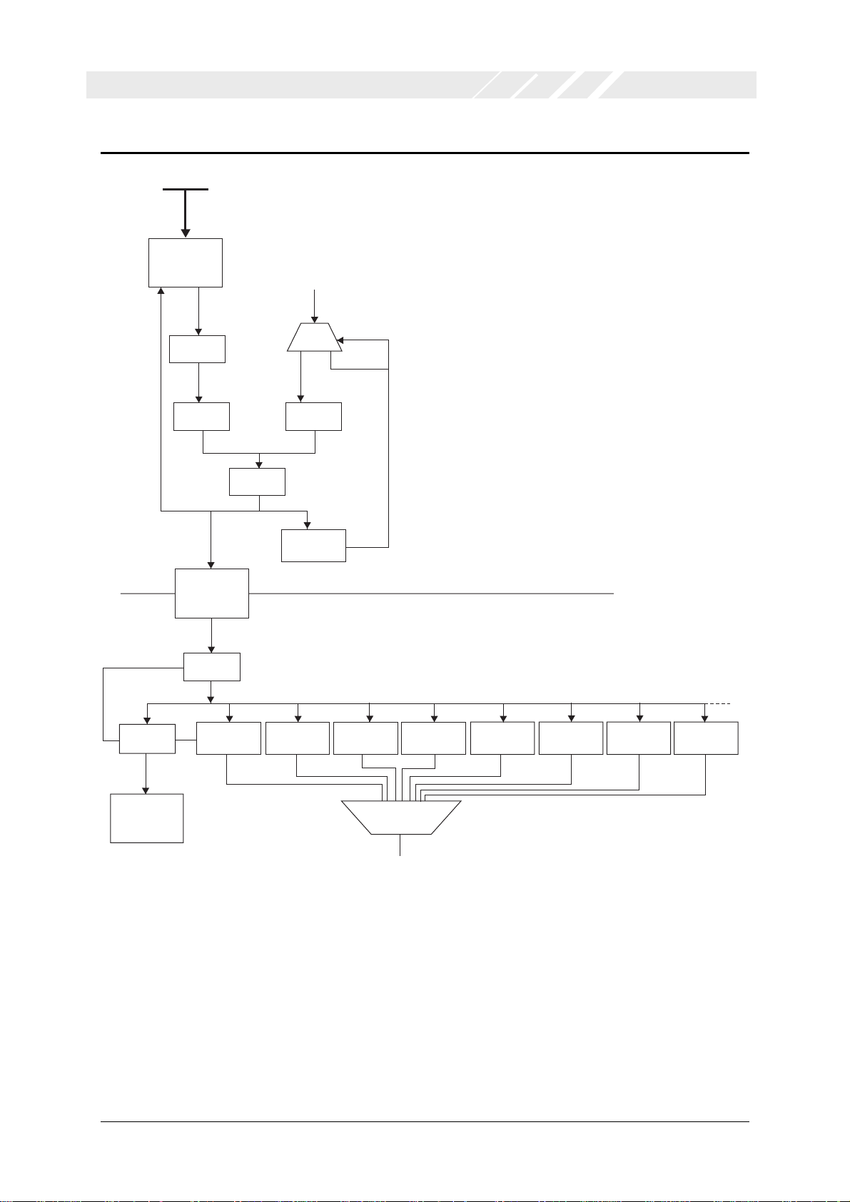
1. BLOCK DIAGRAM
PCI Bus
PCI
Interface
32-bit - 8-bit
Bridge
EEPROM
Signals
OX16PCI958 DATA SHEET
Local Side
Configuration
Registers
UART RAM
Blocks
Address
Encode
Arbiter
Asynchronous
Bridge
Address
Decode
UART UART
EEPROM
Reader
PCI Side
Configuration
Registers
UART UART
PCI Clock Domain
Local Clock Domain
I/O
Switching
UART UART UART UART
I/O Banks
Note: The connections between the UART RAM blocks and each of the UARTs are omitted for clarity.
DS-0022 Nov 05 External—Free Release Page 3

OXFORD SEMICONDUCTOR LTD.
2. PIN INFORMATION—160-PIN QFP
2.1. Pinout
SOUT1
DSR2
SIN2
RTS2
VSS
SOUT2
CTS2
DTR2
RI2
VDD
DCD3
DSR3
SIN3
RTS3
VSS
SOUT33
CTS3
DTR3
VDD
LINEDRIVER_EN
RI3
VDD
VSS
INTA#
RST#
CLK
PME#
VDDP
AD31
AD30
AD29
VSS
AD28
AD27
AD26
AD25
VDDP
AD24
VSS
C/BE#3
IDSEL
CTS1
DTR1
RI1
VDD
DCD2
116
117
118
119
120
121
122
123
124
125
126
127
128
129
130
131
132
133
134
135
136
137
138
139
140
141
142
143
144
145
146
147
148
149
150
151
152
153
154
155
156
157
158
159
160
12345678910111213141516171920212223242526272829303132
VSS
115
SIN1
RTS1
112
113
114
RI0
108
DTR1
107
106
CTS0
105
104
103
VDD
102
101
100
98
99
VDD
111
DCD1
DSR1
110
109
SIN0
DCD4
DCD0
DSR0
RTS0
SOUT0
VSS
OX16PCI958
18
OX16PCI958 DATA SHEET
RTS4
VSS
DSR4
97
969594939291908988878685848382
SIN4
VDD
SOUT4
CTS4
DTR4
RI4
DCD5
VSS
33343536373839
DSR5
SIN5
VDD
RTS5
NC
SOUT5
81
80
79
78
77
76
75
74
73
72
71
70
69
68
67
66
65
64
63
62
61
60
59
58
57
56
55
54
53
52
51
50
49
48
47
46
45
44
43
42
41
40
CTS5
XTALO
XTALI
VSS
DTR5
RI5
VDD
DCD6
DSR6
SIN6
RTS6
VSS
SOUT6
CTS6
DTR6
VDD
RI6
DCD7
DSR7
SIN7
VSS
RTS7
SOUT7
CTS7
VDD
DTR7
RI7
EECS
EECK
VSS
EEDIO
MODE0
TESTN
VDDP
VDD
AD0
AD1
AD2
VSS
AD3
AD23
AD22
VDDP
AD21
AD20
VSS
AD19
AD18
AD17
AD16
VDDP
C/BE#2
VSS
IRDY#
FRAME#
TRDY#
DEVSEL#
STOP#
VDDP
PERR#
PAR
SERR#
VSS
C/BE#1
AD15
AD14
AD13
AD12
AD11
VDDP
AD10
AD9
VSS
AD8
AD7
C/BE#0
AD6
AD5
VDDP
AD4
DS-0022 Nov 05 External—Free Release Page 4

OXFORD SEMICONDUCTOR LTD.
OX16PCI958 DATA SHEET
2.2. Pin Descriptions
Table 1 lists the pin allocations, names and describes them.
Table 1 Pin Descriptions
Name Pin Dir Description
PCI bus signals
PAR 22 IO
CLK 145 I
RST# 144 I
FRAME# 13 I
IRDY# 14 I
TRDY# 16 OT
DEVSEL# 17 OT
STOP# 18 OT
PERR# 19 OT
SERR# 21 OT
INTA# 143 OT
PME# 146 OT
IDSEL 160 I
148, 149,150, 152, 153, 154, 155, 157, 1, 3, 4, 5, 7, 8, 9, 10,
AD[31:0]
25, 26, 27, 28, 30, 31, 32, 34, 36, 37, 39, 40, 41, 43, 44, 45
IO
C/BE#3 159 I
C/BE#2 12 I
C/BE#1 23 I
C/BE#0 35 I
Chip configuration
EECS 53 O
EECK 52 O
EEDIO 50 IO
Local clock
XTALI 78 I
XTALO 79 O
Local side
LD_EN 140 O
Power and ground
VSS (GND) 6, 15, 24, 33, 42, 49, 51, 60, 69, 77, 88, 97, 106, 115, 124, 134, 142, 151, 158
VDD (5V) 56, 65, 74, 84, 93, 102, 111, 120, 129, 138
VDDP 2, 11, 20, 29, 38, 46, 47, 141, 147, 156
The VDDP pins provide power to the PCI I/O buffers, and must be connected to the +V
on the PCI connector.
Table 2 &
pins
I/O
DS-0022 Nov 05 External—Free Release Page 5

OXFORD SEMICONDUCTOR LTD.
Table 3 list pin allocations for the local I/O banks.
Table 2 Local I/O Bank 0—3 Pin Allocations
OX16PCI958 DATA SHEET
Table 3 Local I/O Bank 4—7 Pin Allocations
IO# Bank Pin Dir Name
0 0 99 I DCD
1 100 I DSR
2 101 I SIN
3 103 O RTS
4 104 O SOUT
5 105 I CTS
6 107 O DTR
7 108 I RI
0 1 109 I DCD
1 110 I DSR
2 112 I SIN
3 113 O RTS
4 114 O SOUT
5 116 I CTS
6 117 O DTR
7 118 I RI
0 2 119 I DCD
1 121 I DSR
2 122 I SIN
3 123 O RTS
4 125 O SOUT
5 126 I CTS
6 127 O DTR
7 128 I RI
0 3 130 I DCD
1 131 I DSR
2 132 I SIN
3 133 O RTS
4 135 O SOUT
5 136 I CTS
6 137 O DTR
7 139 I RI
IO# Bank Pin Dir Name
0 4 98 I DCD
1 96 I DSR
2 95 I SIN
3 94 O RTS
4 92 O SOUT
5 91 I CTS
6 90 O DTR
7 89 I RI
0 5 87 I DCD
1 86 I DSR
2 85 I SIN
3 83 O RTS
4 82 O SOUT
5 80 I CTS
6 76 O DTR
7 75 I RI
0 6 73 I DCD
1 72 I DSR
2 71 I SIN
3 70 O RTS
4 68 O SOUT
5 67 I CTS
6 66 O DTR
7 64 I RI
0 7 63 I DCD
1 62 I DSR
2 61 I SIN
3 59 O RTS
4 58 O SOUT
5 57 I CTS
6 55 O DTR
7 54 I RI
DS-0022 Nov 05 External—Free Release Page 6

OXFORD SEMICONDUCTOR LTD.
OX16PCI958 DATA SHEET
3. PCI INTERFACE
The PCI interface conforms to revisions 2.1, 2.2, 2.3 and 3.0 of the PCI Specification, and version 1.1
of the PCI Power Management Specification.
Six base address registers are implemented in the OXPCI958:
• BAR0—128-byte memory-mapped region
• BAR1—128-byte I/O-mapped region
• BAR2—64-byte I/O-mapped region
• BAR3—16-byte I/O-mapped region
• BAR4—64-byte memory-mapped region
• BAR5—16-byte memory-mapped region
All memory regions are in 32-bit address space, and are marked as non-prefetchable.
3.1. Internal Address Map
The internal address map is referenced by the EEPROM to configure the UARTs. Table 4 shows how
PCI accesses are mapped to internal addresses:
Table 4 PCI Address Mapping
PCI side
BAR0, 1
local side
configuration
BAR2, 4 local functions UARTs 80h to BFh
BAR3, 5 local functions SISR C0h to CFh
Notes:
• Addresses in the range 40h-7Fh are aliased with a period of 32, i.e., address bit 5 is not decoded
in this range
• Addresses in the range C0h-FFh are aliased with a period of 16, i.e., address bits 5:4 are not
decoded in this range. For example, if BAR4 is configured as C8000400h, a memory access at
C8000413h, which is BAR4+13h, would access internal address 80h+13h = 93h
• The serial EEPROM reader can access any internal address
Table 5 lists the PCI register offsets.
PCI bridge configuration 00h to 2Fh
EEPROM control, power management 30h to 3Fh
UART, SISR 40h to 7Fh
DS-0022 Nov 05 External—Free Release Page 7

OXFORD SEMICONDUCTOR LTD.
BAR Internal address Use
BAR0, 1
00h – 19h PCI setup registers, as described in section 3.4.
30h EEPROM-control register
31h Power-management control register
34h UART interrupt status
35h
40h UART-enable register
41h UART IO bank switching/rotation
42h SISR enable register
4Ch UART configuration
50h Global UART clock pre-divider
BAR2,4
80h-87h UART 0 registers 0-7
88h-8Fh UART 1 registers 0-7
90h-97h UART 2 registers 0-7
98h-9Fh UART 3 registers 0-7
A0h-A7h UART 4 registers 0-7
A8h-AFh UART 5 registers 0-7
B0h-B7h UART 6 registers 0-7
B8h-BFh UART 7 registers 0-7
BAR3,5
C0h SISR, if SISR enabled
C0h-C1h UART 0 registers 8-9, if SISR not enabled
C2h-C3h UART 1 registers 8-9
C4h-C5h UART 2 registers 8-9
C6h-C7h UART 3 registers 8-9
C8h-C9h UART 4 registers 8-9
CAh-CBh UART 5 registers 8-9
CCh-CDh UART 6 registers 8-9
CEh-CFh UART 7 registers 8-9
other RFU
OX16PCI958 DATA SHEET
Table 5 Register Offsets
Notes:
• Writes to undefined internal addresses are ignored, and reads from undefined internal addresses
return zero
• For shared address ranges, the SISR takes priority over the UARTs
DS-0022 Nov 05 External—Free Release Page 8

OXFORD SEMICONDUCTOR LTD.
OX16PCI958 DATA SHEET
3.2. Configuration & Control Registers
Table 6 summarizes the configuration and control registers for quick reference.
Table 6 Configuration & Control Register Summary
A use D7 D6 D5 D4 D3 D2 D1 D0
EEDIO
output
enable
EEDIO
data out
30h
EEPROMcontrol register
EET2 EET1 RFU
EEDIO
data in
EECS EECK
Power-
31h
management
RFU PM_DRIVER PM_LCLK PM_OSC
control register
UART interrupt
34h
40h
status (RO)
UART-enable
register
U7INT U6INT U5INT U4INT U3INT U2INT U1INT U0INT
U7EN U6EN U5EN U4EN U3EN U2EN U1EN U0EN
42h SISR enable SEN RFU
UART
4Ch
50h
configuration
Global predivider
RFU 1b RFU
RFU1 RFU1 GCS1 RFU1 RFU GCS0 RFU1 RFU
EEPROM-Control Register
The OX16PCI958 automatically takes control of the EECS, EECK and EEDIO pins after a deassertion
of the host bus RESET signal, in order to read in configuration data. Afterwards, the signals may be
controlled though accesses to this register.
Field (Bits) Description
EET2 (7) High—at least 70 PCI clock cycles have occurred since the register was last written.
Cleared when the register is written. Set to the value of EET1 every 70th PCI clock cycle.
This may be useful for ensuring that EEPROM timing constraints are met
EET1 (6) Cleared when the register is written. Set every 70th PCI clock cycle
EEDIO data in (4) Returns the current logic level on the EEDIO pin.
EECS (3) Controls EECS output.
EECK (2) Controls EECK output
EEDIO output
enable (1)
EEDIO data out (0) Controls the logic level driven onto EEDIO when bit 1 is set.
This register is set to 00h on a PCI reset.
1—the value last written to bit 0 is driven on the EEDIO pin
0—EEDIO pin is tri-stated
DS-0022 Nov 05 External—Free Release Page 9

OXFORD SEMICONDUCTOR LTD.
OX16PCI958 DATA SHEET
Power-Management Control Register
Each two-bit group represents a powermanagement level range, as shown in Table 7,
defining whether an element is disabled, which
is shown in Table 8.
Table 7 Power Management Group
Field (Bits) Control Measure
PM_DRIVER driver_en output deasserted
PM_LCLK Local-side clock gated off
PM_OSC Local-side oscillator disabled
Table 8 Element Disabling
Value Description
0 0 Never disabled
0 1 Disabled in D1, D2 & D3
1 0 Disabled in D2 and D3
1 1 Disabled in D3 only
This register is set to 00h on a PCI reset.
UART Interrupt State
Each bit in this read-only register reports the
interrupt status of the corresponding internal
UART.
Global UART Clock Pre-Divider
This register sets a pre-division value for all
the internal UARTs.
Bit 5—One of the clock pre-division factors,
see Table 9
Bit 2—One of the clock pre-division factors,
see Table 9
After a reset, this register is set to F6h, giving
a divide-by-8 clock setting for all UARTs. For
the standard 14.7456 MHz external crystal,
this gives a 1.8432 MHz effective clock to the
UARTs.
For backwards compatibility, write only one of
the four values in Table 9 to bits 5 and 2:
Table 9 Clock Pre-Division Values
Value Divisor
F6h 8
F2h 4
D6h 2
D2h 1
The above register settings are recommended
for backwards compatibility, but Table 10
shows how the actual control logic operates.
Table 10 Clock Division Logic
UART Enable
Each bit in this register enables the
corresponding internal UART to be accessed
on the internal bus, by either the PCI interface
or the EEPROM reader.
SISR Enable
Bit 7 must be set to enable access to the
shared interrupt status register (SISR).
This register is set to 80h on a PCI reset.
UART Configuration
Bit 5 must be set to binary 1 to ensure correct
operation of the UART
GCS1 GCS0 Division
1 1 8
1 0 4
0 1 2
0 0 1
DS-0022 Nov 05 External—Free Release Page 10

OXFORD SEMICONDUCTOR LTD.
OX16PCI958 DATA SHEET
3.3. PCI Configuration Space Registers
The PCI interface presents a type 0 configuration register set in configuration space, with the
standard extension for power management. Table 11 summarizes the PCI configuration space
registers.
Table 11 PCI Configuration Space Registers
Configuration register Address
Offset
00h Device ID Vendor ID
04h Status Command
08h Class code Revision ID
0Ch BIST Header type Latency timer Cache line size
10h Base address register 0 (BAR0)
14h Base address register 1 (BAR1)
18h Base address register 2 (BAR2)
1Ch Base address register 3 (BAR3)
20h Base address register 4 (BAR4)
24h Base address register 5 (BAR5)
28h Cardbus CIS pointer
2Ch Subsystem device ID Subsystem vendor ID
30h Expansion ROM base address register
34h RFU Capabilities pointer
38h RFU
3Ch Max_lat Min_gnt Interrupt pin Interrupt line
40h Power management capabilities (PMC) Next Ptr (always 0) Cap_ID (always 0)
44h PM_Data PMCSR_BSE PMC Control/Status register (PMCSR)
31 24 23 16 15 8 7 0
Device ID Register
This register is read-only via configuration
accesses, and returns the current value of the
DID register (see section 3.4 for details of this
and other PCI set-up registers).
Vendor ID Register
This register is read-only via configuration
accesses, and returns the current value of the
VID register.
Status Register
This register records information on the PCI
interface state, as described in the PCI
specification.
Write 1 to bits 11, 14 and 15 to clear them, all
others are read-only.
Bits Description
15 1—parity error, even if parity error
handling is disabled by bit 6 in the
Command register
14 Set whenever the device asserts SERR#.
13 0
12 0
11 Set whenever the device terminates a
transaction with Target-Abort.
10:9 Device select timing. Target access
timing of the function via the DEVSEL#
output. This device is a medium speed
target device (01b)
8 0
7 0
5 0
4 1
3 Reflects the interrupt state in the
device/function. INTA# is only asserted
when the Interrupt Disable bit in
Command is 0 & this Interrupt Status bit
is a 1. Setting the Interrupt Disable bit to
a 1 has no effect on the state of this bit.
DS-0022 Nov 05 External—Free Release Page 11

OXFORD SEMICONDUCTOR LTD.
Command Register
OX16PCI958 DATA SHEET
Latency Timer
This register enables certain features of the
PCI interface.
Bits Description
10 1—disables INTA# assertion
0—enables INTA# assertion
After RST# is 0
9 0
8 1—enables. the function to report
address parity errors via SERR#
7 0
6 1—enables the function to report parity
errors via PERR#
5 0
4 0
3 0
2 0
1 Controls the response to memory space
accesses.
1—allows the device respond to the PCI
bus memory accesses as a target
0 Controls the response to I/O accesses.
1—allows the device respond to the PCI
bus I/O accesses as a target
Read-only register always returns 00h. (Not
relevant for target-only PCI devices).
Cache Line Size
This register is read-only and always returns
00h. (The device does not support cache line
wrap mode)
Base Address Register 0
This register sets the PCI base address in
memory space for access to local
configuration registers. The register has bits
31-7 writable, and the remainder of the bits are
always 0. This forms a request for 128 bytes of
memory space with a 32-bit address, marked
as non-prefetchable. Accesses made to the
memory range defined by this BAR map to
internal configuration registers at internal
addresses 00h-07h.
Base Address Register 1
Class-Code Register
This register is read-only via configuration
accesses, and returns the current value of the
PCC register.
Revision ID Register
This register is read-only via configuration
accesses, and returns the current value of the
REV register.
BIST Register
This byte always returns 00h, and writes to the
byte are ignored, as there is no BIST function.
Header Type
This byte always returns 00h, indicating a type
0 header and a single-function device. Writes
to the byte are ignored.
This register sets the PCI base address in I/O
space for access to local configuration
registers. The register has bits 31:7 writable;
the remainder are always 01h. This forms a
request for 128 bytes of I/O space. Accesses
made to the I/O range defined by this BAR
map to internal configuration registers at
internal addresses 00h-07h.
Base Address Register 2
This base address register is for a mapping of
64 bytes in I/O space. Accesses made to the
I/O range defined by this BAR map to internal
UARTs at internal addresses 80h-BFh.
Base Address Register 3
This base address register is for a mapping of
16 bytes in I/O space. Accesses made to the
I/O range defined by this BAR map to unused
internal addresses C0h-CFh.
DS-0022 Nov 05 External—Free Release Page 12

OXFORD SEMICONDUCTOR LTD.
Base Address Register 4
OX16PCI958 DATA SHEET
Interrupt Pin Register
This base address register is for a mapping of
64 bytes in 32-bit memory space (nonprefetchable memory). Accesses made to the
memory range defined by this BAR map to
internal UARTs at internal addresses 80h-BFh.
Base Address Register 5
This base address register is for a mapping of
16 bytes in 32-bit memory space (nonprefetchable memory). Accesses made to the
memory range defined by this BAR map to
internal addresses C0h-CFh.
Cardbus CIS Pointer
Hard-wired to zero, as this device is not for
use in CardBus applications.
Subsystem Device ID Register
This register is read-only via configuration
accesses, and returns the current value of the
SDID register.
This register is read-only via configuration
accesses, but may be set to either 00h or 01h
using local-register access via BAR0, BAR1 or
EEPROM configuration. It is set to 01h
following a PCI reset.
Interrupt Line Register
This register is read-write accessible via
configuration accesses. It is set to 00h
following a PCI reset.
Power-Management Registers
The Power Management Capabilities register
is read-only via configuration accesses. It
provides the host system with information on
the power-management capabilities of the PCI
device and returns the current value of the
PMC register. It is set to a generic-configured
value following a PCI reset.
This register is mostly just for the passing of
power management information to the host
system, but two of the fields also have an
affect on the operation of the block:
Subsystem Vendor ID register
This register is read-only via configuration
accesses, and returns the current value of the
SVID register.
Expansion ROM Base Address Register
Hard-wired to zero.
Capabilities Pointer
This register is read-only and always returns
40h, as this is where the power management
registers are located.
Max_lat Register
Read-only register which always returns 00h.
(Not relevant for target-only PCI devices)
Bits Description
10 0—writing 10b to the PowerState bits in
PMCSR (see below) leaves PowerState
unchanged
9 0—writing 01b to the PowerState bits in
the PMCSR (see below) leaves
PowerState unchanged
Min_gnt Register
Read-only register which always returns 00h.
(Not relevant for target-only PCI devices)
DS-0022 Nov 05 External—Free Release Page 13

OXFORD SEMICONDUCTOR LTD.
The Power Management Control/Status
register (PMCSR) has a mixture of read-only,
read/write and read/clear-on-write bits.
Bits Description
15 Set when the function would assert the
PME# signal if bit 8 is enabled. Writing
1 clears it & causes the function to stop
asserting PME#. Writing 0 has no
effect.
Cleared on PCI reset
14:13 Read-only scaling factor to be used
when interpreting the value of the
Power Management Data register. The
value and meaning of this field will
depend on which data value has been
selected using bits 12:9
12:9 Read/write field used to select which
data is to be reported through the Data
register & bits 14:13. Resets to 0
8 1—enables PME#
0—disables PME# (default)
1:0 Determines the current power state of a
function & sets it into a new power state
using the values below.
00b—D0
01b—D1
10b—D2
11b—D3
If software attempts to write an
unsupported, optional state to this field
(i.e. D1 when D1_Support is not set, or
D2 when D2_Support is not set), the
write operation completes normally on
the bus; however, the data is discarded
and no state change occurs.
Reset value 00b
OX16PCI958 DATA SHEET
The Power Management Data register at
offset 47h is read-only, and returns a value
which depends on which data value has been
selected using PMCSR [12:9].
The Power Management Bridge Support
Extensions register at offset 46h is read-only,
and always returns the value 00h.
DS-0022 Nov 05 External—Free Release Page 14
 Loading...