

OXFORD OX16PCI954 User Manual

FEATURES
OX16PCI954
Integrated Quad UART
and PCI interface
• Four 16C950 High performance UART channels
• 8/32-bit Pass-through Local Bus
• IEEE1284 EPP parallel port
• Multi-function target PCI controller, fully PCI 2.2 and
PCI Power Management 1.0 compliant
• UARTs fully software compatible with 16C550-type
devices.
• Baud rates up to 15Mbps in asynchronous mode and
60Mbps in external 1x clock mode
• 128-byte deep FIFO per transmitter and receiver
• Flexible clock prescaler from 1 to 31.875
• Automated in-band flow control using programmable
Xon/Xoff in both directions
• Automated out-of-band flow control using CTS#/RTS#
and/or DSR#/DTR#
DESCRIPTION
The OX16PCI954 is a single chip solution for PCI-based
serial and parallel expansion add-in cards. It is a dual
function PCI device, where function 0 offers four ultra-high
performance OX16C950 UARTs, and function 1 is
configurable to offer either an 8 bit Local Bus or a bidirectional parallel port. Serial port cards with up to 8 ports
(or with 4 serial ports and a parallel port) can be designed
without redefining any device or timing parameters.
Each channel in the OX16PCI954, the fastest available
PC-compatible UART, offers data rates up to 15Mbps and
128-deep transmitter and receiver FIFOs. Deep FIFOs
reduce CPU overhead and allow utilisation of higher data
rates. Each channel is software compatible with the widely
used industry-standard 16C550 devices and compatibles
as well as the OX16C95x family of high performance
UARTs. In addition to increased performance and FIFO
size, the UARTs also provide the full set of OX16C95x
enhanced features including automated in-band flow
control, readable FIFO levels etc.
The efficient 32-bit, 33MHz target-only PCI interface is
compliant with version 2.2 of the PCI Bus Specification and
version 1.0 of PCI Power Management Specification. For
applications that do not require the internal parallel port or
the local Bus, card designers can assign a Subsystem
Vendor ID and a Subsystem ID using 32 input pins. If the
UARTs are not required, the Local Bus can be extended
from 8-bit operation to a full 32-bit pass-through interface.
• Arbitrary trigger levels for receiver and transmitter
FIFO interrupts and automatic in-band and out-ofband flow control
• Infra-red (IrDA) receiver and transmitter operation
• 9-bit data framing as well as 5,6,7 and 8
• 12 multi-purpose IO pins which can be configured as
interrupt input pins
• Can be reconfigured using optional non-volatile
configuration memory (EEPROM)
• Global Interrupt Status and readable FIFO levels to
facilitate implementation of efficient device drivers
• Operation via IO or memory mapping.
• Detection of bad data in the receiver FIFO
• 5.0V operation
• 160 TQFP package
For full flexibility, all the default register values can be
overwritten using an optional Microwire
To enhance device driver efficiency and reduce interrupt
latency, internal UARTs have multi-port features such as
shadowed FIFO fill levels, a global interrupt source register
and Good-Data Status, readable in four adjacent DWORD
registers visible to logical functions in IO space and
memory space.
Expansion of serial cards beyond four channels is possible
using the 8-bit pass-through Local Bus function. The
addressable space can be increased up to 256 bytes, and
divided into four chip-select regions. In 32-bit mode the bus
can map up to 16kb of Memory address space. This
flexible expansion scheme caters for cards with up to 20
serial ports using external 16C950, 16C952, 16C954 or
compatible devices, for composite applications such as
combined serial and parallel port expansion cards.
The OX16PCI954 also provides an IEEE1284 EPP parallel
port which fully supports the existing Centronics interface.
The parallel port can be enabled in place of the Local Bus.
TM
serial EEPROM.
Oxford Semiconductor Ltd.
69 Milton Park, Abingdon, Oxon, OX14 4RX, UK
Tel: +44 (0)1235 824900
Fax: +44(0)1235 821141
External—Free Release
© Oxford Semiconductor 2005
DS-0029 Jul 05
Part No. OX16PCI954-TQC60-A1
OX16PCI954-TQA1G

OXFORD SEMICONDUCTOR LTD.
REVISION HISTORY
REV DATE REASON FOR CHANGE / SUMMARY OF CHANGE
Jul 2005 29/07/2005 Revision for additional order code
OX16PCI954
DS-0029 Jul 05 External—Free Release Page 2

OXFORD SEMICONDUCTOR LTD.
OX16PCI954
CONTENTS
FEATURES...................................................................................................................................................1
DESCRIPTION..............................................................................................................................................1
CONTENTS...................................................................................................................................................3
1 PERFORMANCE COMPARISON..........................................................................................................6
2 BLOCK DIAGRAM ................................................................................................................................7
3 PIN INFORMATION...............................................................................................................................8
4 PIN DESCRIPTIONS..............................................................................................................................9
5 CONFIGURATION & OPERATION.....................................................................................................14
6 PCI TARGET CONTROLLER..............................................................................................................15
6.1 OPERATION .....................................................................................................................................................................15
6.2 CONFIGURATION SPACE...............................................................................................................................................15
6.2.1 PCI CONFIGURATION SPACE REGISTER MAP........................................................................................................16
6.3 ACCESSING LOGICAL FUNCTIONS.............................................................................................................................. 17
6.3.1 PCI ACCESS TO INTERNAL UARTS...........................................................................................................................17
6.3.2 PCI ACCESS TO 8-BIT LOCAL BUS............................................................................................................................17
6.3.3 PCI ACCESS TO PARALLEL PORT............................................................................................................................18
6.3.4 PCI ACCESS TO 32-BIT LOCAL BUS..........................................................................................................................18
6.4 ACCESSING LOCAL CONFIGURATION REGISTERS................................................................................................... 19
6.4.1 LOCAL CONFIGURATION AND CONTROL REGISTER ‘LCC’ (OFFSET 0X00)........................................................19
6.4.2 MULTI-PURPOSE I/O CONFIGURATION REGISTER ‘MIC’ (OFFSET 0X04)............................................................20
6.4.3 LOCAL BUS TIMING PARAMETER REGISTER 1 ‘LT1’ (OFFSET 0X08):..................................................................21
6.4.4 LOCAL BUS TIMING PARAMETER REGISTER 2 ‘LT2’ (OFFSET 0X0C):.................................................................23
6.4.5 UART RECEIVER FIFO LEVELS ‘URL’ (OFFSET 0X10).............................................................................................24
6.4.6 UART TRANSMITTER FIFO LEVELS ‘UTL’ (OFFSET 0X14)......................................................................................24
6.4.7 UART INTERRUPT SOURCE REGISTER ‘UIS’ (OFFSET 0X18)...............................................................................25
6.4.8 GLOBAL INTERRUPT STATUS AND CONTROL REGISTER ‘GIS’ (OFFSET 0X1C)...............................................26
6.5 PCI INTERRUPTS.............................................................................................................................................................27
6.6 POWER MANAGEMENT..................................................................................................................................................28
6.6.1 POWER MANAGEMENT OF FUNCTION 0.................................................................................................................28
6.6.2 POWER MANAGEMENT OF FUNCTION 1.................................................................................................................29
7 INTERNAL OX16C950 UARTS...........................................................................................................30
7.1 OPERATION – MODE SELECTION.................................................................................................................................30
7.1.1 450 MODE.....................................................................................................................................................................30
7.1.2 550 MODE.....................................................................................................................................................................30
7.1.3 EXTENDED 550 MODE................................................................................................................................................30
7.1.4 750 MODE.....................................................................................................................................................................30
7.1.5 650 MODE.....................................................................................................................................................................30
7.1.6 950 MODE.....................................................................................................................................................................31
7.2 REGISTER DESCRIPTION TABLES...............................................................................................................................32
7.3 RESET CONFIGURATION...............................................................................................................................................35
7.3.1 HARDWARE RESET....................................................................................................................................................35
7.3.2 SOFTWARE RESET.....................................................................................................................................................35
7.4 TRANSMITTER AND RECEIVER FIFOS.........................................................................................................................36
7.4.1 FIFO CONTROL REGISTER ‘FCR’..............................................................................................................................36
7.5 LINE CONTROL & STATUS............................................................................................................................................. 37
7.5.1 FALSE START BIT DETECTION..................................................................................................................................37
DS-0029 Jul 05 External—Free Release Page 3

OXFORD SEMICONDUCTOR LTD.
7.5.2 LINE CONTROL REGISTER ‘LCR’...............................................................................................................................37
7.5.3 LINE STATUS REGISTER ‘LSR’..................................................................................................................................38
7.6 INTERRUPTS & SLEEP MODE........................................................................................................................................39
7.6.1 INTERRUPT ENABLE REGISTER ‘IER’.......................................................................................................................39
7.6.2 INTERRUPT STATUS REGISTER ‘ISR’.......................................................................................................................40
7.6.3 INTERRUPT DESCRIPTION........................................................................................................................................40
7.6.4 SLEEP MODE...............................................................................................................................................................41
7.7 MODEM INTERFACE.......................................................................................................................................................41
7.7.1 MODEM CONTROL REGISTER ‘MCR’........................................................................................................................41
7.7.2 MODEM STATUS REGISTER ‘MSR’...........................................................................................................................42
7.8 OTHER STANDARD REGISTERS...................................................................................................................................42
7.8.1 DIVISOR LATCH REGISTERS ‘DLL & DLM’................................................................................................................42
7.8.2 SCRATCH PAD REGISTER ‘SPR’...............................................................................................................................42
7.9 AUTOMATIC FLOW CONTROL.......................................................................................................................................43
7.9.1 ENHANCED FEATURES REGISTER ‘EFR’.................................................................................................................43
7.9.2 SPECIAL CHARACTER DETECTION..........................................................................................................................44
7.9.3 AUTOMATIC IN-BAND FLOW CONTROL...................................................................................................................44
7.9.4 AUTOMATIC OUT-OF-BAND FLOW CONTROL.........................................................................................................44
7.10 BAUD RATE GENERATION............................................................................................................................................. 45
7.10.1 GENERAL OPERATION...............................................................................................................................................45
7.10.2 CLOCK PRESCALER REGISTER ‘CPR’......................................................................................................................45
7.10.3 TIMES CLOCK REGISTER ‘TCR’.................................................................................................................................45
7.10.4 EXTERNAL 1X CLOCK MODE.....................................................................................................................................47
7.10.5 CRYSTAL OSCILLATOR CIRCUIT ..............................................................................................................................47
7.11 ADDITIONAL FEATURES................................................................................................................................................47
7.11.1 ADDITIONAL STATUS RE GISTER ‘ASR’....................................................................................................................47
7.11.2 FIFO FILL LEVELS ‘TFL & RFL’...................................................................................................................................48
7.11.3 ADDITIONAL CONTROL REGISTER ‘ACR’.................................................................................................................48
7.11.4 TRANSMITTER TRIGGER LEVEL ‘TTL’......................................................................................................................49
7.11.5 RECEIVER INTERRUPT. TRIGGER LEVEL ‘RTL’......................................................................................................49
7.11.6 FLOW CONTROL LEVELS ‘FCL’ & ‘FCH’....................................................................................................................49
7.11.7 DEVICE IDENTIFICATION REGISTERS......................................................................................................................49
7.11.8 CLOCK SELECT REGISTER ‘CKS’..............................................................................................................................50
7.11.9 NINE-BIT MODE REGISTER ‘NMR’.............................................................................................................................50
7.11.10 MODEM DISABLE MASK ‘MDM’..................................................................................................................................51
7.11.11 READABLE FCR ‘RFC’.................................................................................................................................................51
7.11.12 GOOD-DATA STATUS REGISTER ‘GDS’....................................................................................................................51
OX16PCI954
8 LOCAL BUS ........................................................................................................................................52
8.1 OVERVIEW.......................................................................................................................................................................52
8.2 OPERATION .....................................................................................................................................................................52
8.3 CONFIGURATION & PROGRAMMING............................................................................................................................53
9 BIDIRECTIONAL PARALLEL PORT ..................................................................................................54
9.1 OPERATION AND MODE SELECTION...........................................................................................................................54
9.1.1 SPP MODE...................................................................................................................................................................54
9.1.2 PS2 MODE....................................................................................................................................................................54
9.1.3 EPP MODE...................................................................................................................................................................54
9.1.4 ECP MODE (NOT SUPPORTED).................................................................................................................................54
9.2 PARALLEL PORT INTERRUPT.......................................................................................................................................54
9.3 REGISTER DESCRIPTION............................................................................................................................................... 55
9.3.1 PARALLEL PORT DATA REGISTER ‘PDR’.................................................................................................................55
9.3.2 DEVICE STATUS REGISTER ‘DSR’............................................................................................................................55
9.3.3 DEVICE CONTROL REGISTER ‘DCR’.........................................................................................................................56
9.3.4 EPP ADDRESS REGISTER ‘EPPA’.............................................................................................................................56
9.3.5 EPP DATA REGISTERS ‘EPPD1-4’.............................................................................................................................56
9.3.6 EXTENDED CONTROL REGISTER ‘ECR’...................................................................................................................56
DS-0029 Jul 05 External—Free Release Page 4

OXFORD SEMICONDUCTOR LTD.
OX16PCI954
10 SERIAL EEPROM............................................................................................................................57
10.1 SPECIFICATION............................................................................................................................................................... 57
10.2 EEPROM DATA ORGANISATION...................................................................................................................................57
10.2.1 ZONE0: HEADER.........................................................................................................................................................57
10.2.2 ZONE1: LOCAL CONFIGURATION REGISTERS........................................................................................................58
10.2.3 ZONE2: IDENTIFICATION REGISTERS......................................................................................................................59
10.2.4 ZONE3: PCI CONFIGURATION REGISTERS.............................................................................................................59
11 OPERATING CONDITIONS.............................................................................................................60
12 DC ELECTRICAL CHARACTERISTICS..........................................................................................60
12.1 NON-PCI I/O BUFFERS....................................................................................................................................................60
12.2 PCI I/O BUFFERS............................................................................................................................................................. 61
13 AC ELECTRICAL CHARACTERISTICS..........................................................................................62
13.1 PCI BUS............................................................................................................................................................................62
13.2 LOCAL BUS......................................................................................................................................................................62
13.3 SERIAL PORTS................................................................................................................................................................63
14 TIMING WAVEFORMS.....................................................................................................................64
15 PACKAGE INFORMATION..............................................................................................................71
16 ORDERING INFORMATION............................................................................................................71
NOTES........................................................................................................................................................72
CONTACT DETAILS...................................................................................................................................73
DISCLAIMER..............................................................................................................................................73
DS-0029 Jul 05 External—Free Release Page 5

OXFORD SEMICONDUCTOR LTD.
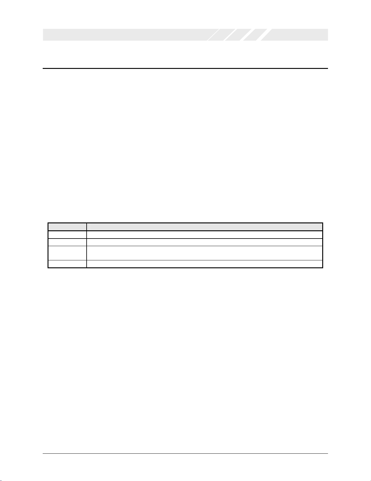
1 PERFORMANCE COMPARISON
Feature
Internal serial channels 4 0 0
Integral 1284 EPP parallel port yes no no
Multi-function PCI device yes no no
Support for PCI Power Management yes no no
Zero wait-state read/write operation yes1 no no
No. of available Local Bus interrupt pins 12 2 2
DWORD access to UART Interrupt Source
Registers & FIFO Levels
Good-Data status yes no no
Full Plug and Play with external EEPROM yes yes yes
Subsystem Vendor ID & Subsystem ID with
no external EEPROM
External 1x baud rate clock yes no no
Max baud rate in normal mode 15 Mbps 115 Kbps 1.5 Mbps
Max baud rate in 1x clock mode 60 Mbps n/a n/a
FIFO depth 128 16 64
Sleep mode yes no yes
Auto Xon/Xoff flow yes no yes
Auto CTS#/RTS# flow yes no yes
Auto DSR#/DTR# flow yes no no
No. of Rx interrupt thresholds 128 4 4
No. of Tx interrupt thresholds 128 1 4
No. of flow control thresholds 128 n/a 4
Transmitter empty interrupt yes no no
Readable status of flow control yes no no
Readable FIFO levels yes no no
Clock prescaler options 248 n/a 2
Rx/Tx disable yes no no
Software reset yes no no
Device ID yes no no
9-bit data frames yes no no
RS485 buffer enable yes no no
Infra-red (IrDA) yes no yes
OX16PCI954
yes no no
yes no no
16C554 +
PLX9050
16C654 +
PLX9050
OX16PCI954
Table 1: OX16PCI950 performance compared with PLX + generic UART combinations
Note 1: Zero wait-state applies only to internal UARTs
Improvements of the OX16PCI954 over discrete solutions:
Higher degree of integration:
OX16PCI954 offers four internal 16C950 high-performance
UARTs and one bi-directional parallel port.
Improved access timing:
Access to internal UARTs require zero or one PCI wait
states. A PCI read transaction from an internal UART can
complete within five PCI clock cycles and a write
DS-0029 Jul 05 External—Free Release Page 6
transaction to an internal UART can complete within four
PCI clock cycles.
Reduces interrupt latency:
OX16PCI954 offers shadowed FIFO levels and Interrupt
status registers of internal UARTs, and Interrupt Status of
internal UARTs and MIO pins to reduce the device driver
interrupt latency.
OXFORD SEMICONDUCTOR LTD.
Power management:
OX16PCI954 complies with PCI Power Management
Specification 1.0 and PC98/99 Power Management
specifications. Both functions offer the extended
capabilities for Power Management. This achieves
significant power saving by enabling device drivers to
power down the PCI function and the channel clock (in
power state D3). Wake-up is requested via PME# from RI
in power-state D3 or any modem line and SIN in powerstate D2.
Optional EEPROM:
OX16PCI954 can be reconfigured from an external
EEPROM. However, this is not required in many
applications as default values are provided for typical
applications up to 8 serial ports, and in some cases the
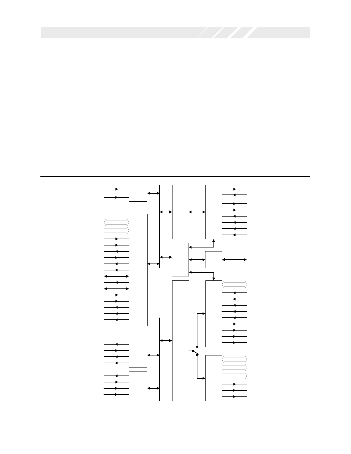
2 BLOCK DIAGRAM
OX16PCI954
Subsystem ID and Subsystem Vendor ID can be set via
input pins.
Multi-function device:
OX16PCI954 is a multi-function device to enable users to
load individual device drivers for internal serial ports, the
internal parallel port and peripheral devices connected to
the Local Bus.
Quad Internal OX16C950 UARTs
OX16PCI954 contains four ultra-high performance UARTs,
which can increase driver efficiency using features such as
128-byte deep transmitter & receiver FIFOs, data rates up
to 60Mbps, flexible clock options, automatic flow control,
programmable interrupt and flow control trigger levels and
readable FIFO levels.
MODE[1:0]
FIFOSEL
AD[31:0]
C/BE[3:0]#
CLK
FRAME#
DEVSEL#
IRDY#
TRDY#
STOP#
PAR
SERR#
PERR#
IDSEL
RST#
INTA#
INTB#
PME#
XTALO
XTALI
UART_Ck_Out
LBCLK
EE_DO
EE_DI
EE_CK
EE_CS
Config.
interface
PCI
interface
Clock &
Baud rate
generator
EEPROM
interface
Internal Data / control bus
Function
0
Interrupt
logic
Function
1
Quad
UARTs
MIO pins
Parallel
port
Local
Bus
SOUT[3:0]
SIN[3:0]
RTS[3:0]#
DTR[3:0]#
CTS[3:0]#
DSR[3:0]#
DCD[3:0]#
RI[3:0]#
MIO[11:0]
PD[7:0]
ACK#
PE
BUSY
SLCT
ERR#
SLIN#
INIT#
AFD#
STB#
LBA[7:0]
LBD[7:0]
LBCS[3:0]
LBWR#
LBRD#
LBRST
Figure 1: OX16PCI954 Block Diagram
DS-0029 Jul 05 External—Free Release Page 7

OXFORD SEMICONDUCTOR LTD.
3 PIN INFORMATION
OX16PCI954
Mode ‘00’: Quad UARTs + 8-bit local bus
LBA1
LBA2
LBA3
LBCS0#
LBCS1#
LBCS2#
LBCS3#
LBRD#
LBWR#
VDD
GND
LBCLK
LBA4
LBA5
LBA6
LBA7
LBA0
LBRST
LBRST#
MIO7
MIO6
MIO5
MIO4
MIO3
MIO2
MIO1
MIO0
INTA#
INTB#
RST#
PME#
AD31
AD30
AD29
AD28
AD27
AD26
AD25
AD24
C/BE3#
IDSEL
AD23
AD22
AD21
AD20
AD19
AD18
121
122
123
124
125
126
127
128
129
130
131
132
133
134
GND
135
CLK
136
VDD
137
138
139
140
141
GND
142
143
144
145
GND
146
VDD
147
148
149
150
151
152
GND
153
154
155
156
VDD
157
GND
158
159
160
VDD
LBDOUT
LBD0
LBD1
LBD2
LBD3
VDD
GND
LBD4
GND
120
119
118
117
116
115
114
113
112
111
110
109
108
107
106
105
104
99989796959493929190898887
102
101
100
103
OX16PCI954-TQC60-A
1234567891011121314151617
GND
AD17
AD16
IRDY#
TRDY#
STOP#
PERR#
SERR#
C/BE2#
FRAME#
DEVSEL#
1920212223242526272829303132333435
18
PAR
VDD
GND
AD12
AD15
AD14
AD13
C/BE1#
AD11
AD8
AD9
VDD
GND
GND
AD10
LBD5
C/BE0#
LBD6
AD7
LBD7
AD6
RI3#
DCD3#
MIO8
MIO9
MIO10
MIO11
SIN3
8584838281
86
3637383940
AD5
AD4
AD3
AD2
VDD
GND
GND
Mode ’10’: Quad UARTs + pin-assignable
Subsystem ID & Subsystem Vendor ID
DSR3#
AD1
CTS3#
AD0
DTR3#
EE_CS
RTS3#
EE_DO
Mode ‘01’: Quad UARTs + parallel port
BUSY
SLCT
ERR#NCNCNCNCNCNC
VDD
GNDNCSLIN#
INIT#
AFD#
STB#
VDD
NC
PD0
PD1
PD2
PD3
VDD
GND
PD4
GND
120
119
118
117
116
115
114
113
112
111
110
109
108
107
106
105
104
PERR#
SERR#
103
18
PAR
VDD
GND
AD15
AD14
AD13
C/BE1#
SOUT3
80
SOUT2
79
RTS2#
78
DTR2#
77
76
CTS2#
DSR2#
75
DCD2#
74
RI2#
73
72
VDD
UART_Ck_Out
71
GND
70
69
SIN2
68
SIN1
RI1#
67
DCD1#
66
65
VDD
64
XTLO
XTLI
63
62
GND
61
DSR1#
60
CTS1#
59
DTR1#
58
RTS1#
57
VDD
56
GND
55
SOUT1
54
SOUT0
53
RTS0#
52
DTR0#
51
CTS0#
50
DSR0#
49
DCD0#
48
RI0#
47
SIN0
46
FIFOSEL
45
Mode0
44
Mode1
43
TEST
42
EE_DI
41
EE_CK
PE
121
ACK#
122
NC
123
MIO7
124
MIO6
125
MIO5
126
MIO4
127
MIO3
128
MIO2
129
MIO1
130
NC
131
INTA#
132
INTB#
133
RST#
134
GND
135
CLK
136
VDD
137
PME#
138
AD31
139
AD30
140
AD29
141
GND
142
AD28
143
AD27
144
AD26
145
GND
VDD
AD25
AD24
C/BE3#
IDSEL
AD23
GND
AD22
AD21
AD20
VDD
GND
AD19
AD18
OX16PCI954-TQC60-A
146
147
148
149
150
151
152
153
154
155
156
157
158
159
160
1234567891011121314151617
GND
AD17
AD16
IRDY#
TRDY#
STOP#
C/BE2#
FRAME#
DEVSEL#
PD5
99989796959493929190898887
102
101
100
1920212223242526272829303132333435
AD8
AD9
VDD
GND
GND
AD12
AD11
AD10
C/BE0#
RI3#
DCD3#
CTS3#
DTR3#
RTS3#
PD6
AD7
DSR3#
PD7
MIO8
MIO9
MIO10
MIO11
SIN3
8584838281
86
3637383940
AD6
AD5
AD4
AD3
AD2
AD1
VDD
GND
GND
SOUT3
80
SOUT2
79
RTS2#
78
DTR2#
77
76
CTS2#
DSR2#
75
DCD2#
74
RI2#
73
72
VDD
NC
71
GND
70
69
SIN2
68
SIN1
RI1#
67
DCD1#
66
65
VDD
64
XTLO
XTLI
63
62
GND
61
DSR1#
60
CTS1#
59
DTR1#
58
RTS1#
57
VDD
56
GND
55
SOUT1
54
SOUT0
53
RTS0#
52
DTR0#
51
CTS0#
50
DSR0#
49
DCD0#
48
RI0#
47
SIN0
46
FIFOSEL
45
Mode0
44
Mode1
43
TEST
42
EE_DI
41
EE_CK
AD0
EE_CS
EE_DO
Mode ‘11’: 32-bit bridge
LBA1
LBA2
LBA3
LBCS0#
LBCS1#
LBCS2#
LBCS3#
LBRD#
LBWR#
VDD
GND
LBCLK
LBA4
LBA5
LBA6
LBA7
Sub_V_ID0
Sub_ID7
Sub_ID6
Sub_ID5
Sub_ID4
Sub_ID3
Sub_ID2
Sub_ID1
Sub_ID0
INTA#
INTB#
PME#
C/BE3#
IDSEL
RST#
AD31
AD30
AD29
AD28
AD27
AD26
AD25
AD24
AD23
AD22
AD21
AD20
AD19
AD18
121
NC
122
NC
123
124
125
126
127
128
129
130
131
132
133
134
GND
135
CLK
136
VDD
137
138
139
140
141
GND
142
143
144
145
GND
146
VDD
147
148
149
150
151
152
GND
153
154
155
156
VDD
157
GND
158
159
160
Sub_ID12
Sub_ID13
Sub_ID14
Sub_ID15NCNC
VDD
GNDNCVDD
NC
VDD
GND
Sub_V_ID1
Sub_V_ID2
Sub_V_ID3
120
119
118
GND
Sub_V_ID8
Sub_V_ID4
Sub_V_ID6
Sub_V_ID5
Sub_V_ID7
117
116
115
114
113
112
111
110
109
108
107
106
105
104
102
101
103
Sub_V_ID15
Sub_V_ID9
Sub_V_ID10
Sub_V_ID11
Sub_V_ID12
Sub_V_ID13
Sub_V_ID154
99989796959493929190898887
100
OX16PCI954-TQC60-A
1234567891011121314151617
GND
AD17
AD16
IRDY#
TRDY#
STOP#
PERR#
C/BE2#
FRAME#
DEVSEL#
SERR#
PAR
GND
AD15
AD14
AD13
C/BE1#
1920212223242526272829303132333435
18
AD9
AD8
AD7
AD6
VDD
VDD
GND
GND
AD12
AD11
AD10
C/BE0#
Sub_ID8
Sub_ID9
VDD
GND
Sub_ID10
Sub_ID11
AD5
AD4
RI3#
SIN3
86
AD3
GND
DCD3#
CTS3#
DSR3#
8584838281
3637383940
AD2
AD1
AD0
DTR3#
EE_CS
RTS3#
EE_DO
VDD
LBDOUT
LBD0
LBD1
LBD2
LBD3
VDD
GND
LBD4
GND
120
119
118
117
116
115
114
113
112
111
110
109
108
107
106
105
104
PERR#
SERR#
103
18
PAR
VDD
GND
AD15
AD14
AD13
C/BE1#
LBA0
SOUT3
80
SOUT2
79
RTS2#
78
DTR2#
77
76
CTS2#
DSR2#
75
DCD2#
74
RI2#
73
72
VDD
NC
71
GND
70
69
SIN2
68
SIN1
67
RI1#
66
DCD1#
65
VDD
64
XTLO
XTLI
63
62
GND
61
DSR1#
60
CTS1#
DTR1#
59
58
RTS1#
57
VDD
56
GND
55
SOUT1
54
SOUT0
53
RTS0#
52
DTR0#
51
CTS0#
50
DSR0#
49
DCD0#
48
RI0#
47
SIN0
46
FIFOSEL
45
Mode0
44
Mode1
43
TEST
42
EE_DI
41
EE_CK
LBRST
LBRST#
MIO7
MIO6
MIO5
MIO4
MIO3
MIO2
MIO1
MIO0
INTA#
INTB#
RST#
PME#
AD31
AD30
AD29
AD28
AD27
AD26
AD25
AD24
C/BE3#
IDSEL
AD23
AD22
AD21
AD20
AD19
AD18
121
122
123
124
125
126
127
128
129
130
131
132
133
134
GND
135
CLK
136
VDD
137
138
139
140
141
GND
142
143
144
145
GND
146
VDD
147
148
149
150
151
152
GND
153
154
155
156
VDD
157
GND
158
159
160
OX16PCI954-TQC60-A
1234567891011121314151617
GND
AD17
AD16
IRDY#
TRDY#
STOP#
C/BE2#
FRAME#
DEVSEL#
LBD5
99989796959493929190898887
102
101
100
1920212223242526272829303132333435
AD8
AD9
VDD
GND
GND
AD10
AD12
AD11
C/BE0#
LBD6
AD7
LBD7
AD6
LBD9
LBD10
LBD12
LBD13
LBD14
LBD11
MIO8
MIO9
MIO10
MIO11
LBD8
8584838281
86
3637383940
AD5
AD4
AD3
AD2
AD1
VDD
GND
GND
LBD15
80
LBA8
79
LBA9
78
LBA10
77
76
LBA11
NC
75
NC
74
NC
73
72
VDD
NC
71
GND
70
69
NC
68
LBD16
LBD17
67
LBD18
66
65
VDD
64
NC
GND
63
62
GND
61
LBD19
60
LBD20
LBD21
59
58
LBD22
57
VDD
56
GND
55
LBD23
54
LBD24
53
LBD25
52
LBD26
51
LBD27
50
LBD28
49
LBD29
48
LBD30
47
LBD31
46
FIFOSEL
45
Mode0
44
Mode1
43
TEST
42
EE_DI
41
EE_CK
AD0
EE_CS
EE_DO
Figure 2: Pinout in all configurable modes (package = 160 TQFP)
DS-0029 Jul 05 External—Free Release Page 8

OXFORD SEMICONDUCTOR LTD.
4 PIN DESCRIPTIONS
OX16PCI954
Mode
00 01 10 11
PCI interface
139, 140, 141, 143, 144, 145, 148,
149, 152, 154, 155, 156, 159, 160,
1, 2, 14, 15, 16, 19, 20, 23, 24, 26,
28, 29, 32, 33, 34, 36, 37, 38
150, 3, 13, 27 P_I C/BE[3:0]# PCI Command/Byte enable
136 P_I CLK PCI system clock
4 P_I FRAME# Cycle Frame
7 P_O DEVSEL# Device Select
5 P_I IRDY# Initiator ready
6 P_O TRDY# Target ready
9 P_O STOP# Target Stop request
12 P_I/O PAR Parity
11 P_O SERR# System error
10 P_I/O PERR# Parity error
151 P_I IDSEL Initialization device select
134 P_I RST# PCI system reset
132,133 P_OD INTA#, INTB# PCI interrupts
138 P_OD PME# Power management event
Serial port pins
46 N/A I FIFOSEL FIFO select. For backward compatibility with 16C550,
80, 79, 55, 54 N/A O SOUT[3:0]
87, 69, 68, 47 N/A I
85, 74, 66, 49 N/A I DCD[3:0]# Active-low modem data-carrier-detect input
82, 77, 59, 52 N/A O
Dir1 Name Description
P_I/O AD[31:0] Multiplexed PCI Address/Data bus
16C650 and 16C750 devices the UARTs’ FIFO depth is 16
when FIFOSEL is low. The FIFO size is increased to 128
when FIFOSEL is high. The unlatched state of this pin is
readable by software. The FIFO size may also be set to 128
by setting FCR[5] when LCR[7] is set, or by putting the
device into enhanced mode.
UART serial data outputs
IrDA_Out[3:0]
SIN[3:0]
I
IrDA_In[3:0]
DTR[3:0]#
485_En[3:0]
O
Tx_Clk_Out[3:0]
O
UART IrDA data output when MCR[6] of the corresponding
channel is set in enhanced mode
UART serial data inputs
UART IrDA data input when IrDA mode is enabled (see
above)
Active-low modem data-terminal-ready output. If automated
DTR# flow control is enabled, the DTR# pin is asserted and
deasserted if the receiver FIFO reaches or falls below the
programmed thresholds, respectively.
In RS485 half-duplex mode, the DTR# pin may be
programmed to reflect the state of the the transmitter empty
bit to automatically control the direction of the RS485
transceiver buffer (see register ACR[4:3])
Transmitter 1x clock (baud rate generator output). For
isochronous applications, the 1x (or Nx) transmitter clock
may be asserted on the DTR# pins (see register CKS[5:4])
DS-0029 Jul 05 External—Free Release Page 9

OXFORD SEMICONDUCTOR LTD.
OX16PCI954
Mode
Dir1 Name Description
00 01 10 11
Serial port pins
81, 78, 58, 53 N/A O RTS[3:0]# Active-low modem request-to-send output. If automated
RTS# flow control is enabled, the RTS# pin is deasserted
and reasserted whenever the receiver FIFO reaches or falls
below the programmed thresholds, respectively.
83, 76, 60, 51 N/A I CTS[3:0]# Active-low modem clear-to-send input. If automated CTS#
flow control is enabled, upon deassertion of the CTS# pin,
the transmitter will complete the current character and enter
the idle mode until the CTS# pin is reasserted. Note: flow
control characters are transmitted regardless of the state of
the CTS# pin.
84, 75, 61, 50 N/A I
I
DSR[3:0]#
Rx_Clk_In[3:0]
Active-low modem data-set-ready input. If automated DSR#
flow control is enabled, upon deassertion of the DSR# pin,
the transmitter will complete the current character and enter
the idle mode until the DSR# pin is reasserted. Note: flow
control characters are transmitted regardless of the state of
the DSR# pin
External receiver clock for isochronous applications. The
Rx_Clk_In is selected when CKS[1:0] = ‘01’.
86, 73, 67, 48 N/A I
I
RI[3:0]#
Tx_Clk_In[3:0]
Active-low modem Ring-Indicator input
External transmitter clock. This clock can be used by the
transmitter (and indirectly by the receiver) when CKS[6]=’1’.
64 N/A O XTLO Crystal oscillator output
63 N/A I XTLI Crystal oscillator input or external clock pin. Maximum
frequency 60MHz
8-bit local bus
71 N/A O UART_Clk_Out Buffered crystal output. This clock can drive external UARTs
122 N/A O LBRST Local bus active-high reset
123 N/A O LBRST# Local bus active-low reset
102 N/A O LBDOUT Local bus data out enable. This pin can be used by external
109 N/A O LBCLK Buffered PCI clock. Can be enabled / disabled by software
114-7 N/A O
112 N/A O
113 N/A O
105-8
118-21
92-5
98-101
N/A O LBA[7:0] Local bus address signals
N/A
See
32-bit
Local
bus
connected to the local bus. Can be enabled / disabled by
software.
transceivers; it is high when LBD[7:0] are in output mode and
low when they are in input mode.
O
O
Z
LBCS[3:0]#
LBDS[3:0]#
LBWR#
LBRDWR#
LBRD#
Hi-Z
Local bus active-low Chip-Select (Intel mode)
Local bus active-low Data-Strobe (Motorola mode)
Local Bus active-low write-strobe (Intel mode)
Local Bus Read-not-Write control (Motorola mode)
Local Bus active-low read-strobe (Intel mode)
Permanent high impedance (Motorola mode)
I/O LBD[7:0] Local bus data signals
DS-0029 Jul 05 External—Free Release Page 10

OXFORD SEMICONDUCTOR LTD.
OX16PCI954
Mode
Dir1 Name Description
00 01 10 11
Parallel port
N/A 122 N/A I
ACK#
I
INTR#
Acknowledge (SPP mode). ACK# is asserted (low) by the
peripheral to indicate that a successful data transfer has
taken place.
Identical function to ACK# (EPP mode).
N/A 121 N/A I PE Paper Empty. Activated by printer when it runs out of paper.
N/A 120 N/A I
N/A 108 N/A OD
I
O
BUSY
WAIT#
SLIN#
ADDRSTB#
Busy (SPP mode). BUSY is asserted (high) by the peripheral
when it is not ready to accept data
Wait (EPP mode). Handshake signal for interlocked IEEE
1284 compliant EPP cycles.
Select (SPP mode). Asserted by host to select the peripheral
Address strobe (EPP mode) provides address read and write
strobe
N/A 119 N/A I SLCT Peripheral selected. Asserted by peripheral when selected.
N/A 118 N/A I ERR# Error. Held low by the peripheral during an error condition.
N/A 107 N/A OD
N/A 106 N/A OD
N/A 105 N/A OD
O
O
O
INIT#
INIT#
AFD#
DATASTB#
STB#
WRITE#
Initialize (SPP mode). Commands the peripheral to initialize.
Initialize (EPP mode). Identical function to SPP mode.
Auto Feed (SPP mode, open-drain)
Data strobe (EPP mode) provides data read and write strobe
Strobe (SPP mode). Used by peripheral to latch data
currently available on PD[7:0]
Write (EPP mode). Indicates a write cycle when low and a
read cycle when high
N/A Bus N/A I/O PD[7:0] Parallel data bus
32-bit Local bus
N/A N/A 122 O LBRST Local bus active-high reset
N/A N/A 123 O LBRST# Local bus active-low reset
N/A N/A 102 O LBDOUT Local bus data out enable. This pin can be used by external
See
8-bit
local
bus
N/A N/A 109 O LBCLK Buffered PCI clock. Can be enabled / disabled by software
N/A N/A 114-7 O O LBCS[3:0]#
LBDS[3:0]#
N/A N/A 112 O
O
LBWR#
LBRDWR#
N/A N/A 113 O Z LBRD#
transceivers; it is high when LBD[7:0] are in output mode and
low when they are in input mode.
Local bus active-low Chip-Select (Intel mode)
Local bus active-low Data-Strobe (Motorola mode)
Local Bus active-low write-strobe (Intel mode)
Local Bus Read-not-Write control (Motorola mode)
Local Bus active-low read-strobe (Intel mode)
N/A N/A
N/A N/A
76-9,
105-8,
118-121
47-55,
58-61,
66-68,
80-87,
92-95,
98-101
Hi-Z
O LBA[12:0] Local bus address signals
I/O LBD[31:0] Local bus data signals
Permanent high impedance (Motorola mode)
DS-0029 Jul 05 External—Free Release Page 11

OXFORD SEMICONDUCTOR LTD.
OX16PCI954
Mode
Dir1 Name Description
00 01 10 11
Subsystem ID & Subsystem Vendor ID pins
N/A
N/A
131-124,
117-114,
91-88
121-118,
108-105,
101-98,
95-92
N/A I Sub_ID[15:0] Subsystem ID. After reset the subsystem ID of Function 0
will default to the value assigned to these pins
N/A I Sub_V_ID[15:0] Subsystem Vendor ID. After reset the subsystem vendor ID
of Function 0 will default to the value assigned to these pins.
Multi-purpose & External interrupt pins
131
N/A
130 130 N/A 130 I/O
129 129 N/A 129 I/O
N/A
131
N/A
N/A
131
N/A
I/O
MIO0
Z
Hi-Z
MIO1
Z
Hi-Z
MIO2
I
PME_In
Multi-purpose I/O 0. Can drive high or low, or assert a PCI
interrupt
Permanent high impedance
Multi-purpose I/O 1. Can drive high or low, or assert a PCI
interrupt
Permanent high-impedance when LCC[6:5] ≠ ‘00’
Multi-purpose I/O 2. When LCC[7] = 0, this pin can drive high
or low, or assert a PCI interrupt.
Input power management event. When LCC[7] is set this
input pin can assert a function 1 PME#
124-128
88-91
N/A 124-8,
88-91
I/O MIO[3:11] Multi-purpose I/O pins. Can drive high or low, or assert a PCI
interrupt
EEPROM pins
41 O EE_CK EEPROM clock
39 O EE_CS EEPROM active-high Chip Select
42 IU EE_DI EEPROM data in. When the serial EEPROM is connected,
this pin should be pulled up using 1-10k resistor. When the
EEPROM is not used the internal pullup is sufficient.
40 O EE_DO EEPROM data out.
Miscellaneous pins
43 IU TEST Must be connected to GND
44,45 I Mode[1:0] Mode selector:
00: Function 0 is Quad UART, Function 1 is 8-bit local bus
01: Function 0 is Quad UART, Function 1 is parallel port
10: Function 0 is Quad UART, Function 1 is unusable as the
local bus pins are used to assign Subsystem ID and
Subsystem Vendor ID to function 0
11: Function 0 is unusable, Function 1 is 32-bit local bus
Power and ground2
18, 31, 57, 72, 97, 111, 147, 157 V AC VDD Supplies power to output buffers in switching (AC) state
22, 65, 104, 137 V DC VDD Power supply. Supplies power to core logic, input buffers
and output buffers in steady state
8, 17, 25, 30, 35, 56, 70, 96, 110,
G AC GND Supplies GND to output buffers in switching (AC) state
142, 146, 153, 158
21, 62, 103, 135 G DC GND Ground (0 volts). Supplies GND to core logic, input buffers
and output buffers in steady state
Table 2: Pin Descriptions
DS-0029 Jul 05 External—Free Release Page 12

OXFORD SEMICONDUCTOR LTD.
Note 1: Direction key:
I Input
IU Input with internal pull-up
O Output
I/O Bi-directional
OD Open drain
NC No connect
Z High impedance
Note 2: Power & Ground
There are two GND and two VDD rails internally. One set of rails supply power and ground to output buffers while in switching
state (called AC power) and another rail supply the core logic, input buffers and output buffers in steady-state (called DC rail).
The rails are not connected internally. This precaution reduces the effects of simultaneous switching outputs and undesirable RF
radiation from the chip. Further precaution is taken by segmenting the GND and VDD AC rails to isolate the PCI, Local Bus and
UART pins.
P_I PCI input
P_O PCI output
P_I/O PCI bi-directional
P_OD PCI open drain
G Ground
V 5.0V power
OX16PCI954
DS-0029 Jul 05 External—Free Release Page 13
OXFORD SEMICONDUCTOR LTD.
5 CONFIGURATION & OPERATION
OX16PCI954
The OX16PCI954 is a multi-function, target-only PCI
device, compliant with the PCI Local Bus Specification,
Revision 2.2 and PCI Power Management Specification,
Revision 1.0.
The OX16PCI954 affords maximum configuration flexibility
by treating the internal UARTs, Local bus and the parallel
port as separate logical functions. Each function has its
own configuration space and is therefore recognised and
configured by the PCI BIOS seperately. The functions
used are configured by the Mode[1:0] pins as shown in
Table 3.
The OX16PCI954 is configured by system start-up
software during the bootstrap process that follows bus
reset. The system scans the bus and reads the vendor and
device identification codes from any devices it finds. It then
loads device-driver software according to this information
and configures the I/O, memory and interrupt resources.
Mode [1:0] Configuration
00 Function 0 is Quad UART, Function 1 is 8-bit local bus
01 Function 0 is Quad UART, Function 1 is parallel port
10 Function 0 is Quad UART, Function 1 is unusable as the local bus pins are used to assign Subsystem
ID and Subsystem Vendor ID to function 0
11 Function 0 is unusable, Function 1 is 32-bit local bus
Device drivers can then access the functions at the
assigned addresses in the usual fashion, with the improved
data throughput provided by PCI.
Each function operates as though it was a separate device;
however there are a set of Local configuration registers
that can be used to enable signals and interrupts, configure
timings, and improve the efficiency of multi-port drivers.
This architecture enables separate drivers to be installed
for each function. Generic port drivers can be hooked to
use the functions individually, or more efficient multi-port
drivers can hook both functions, accessing the Local
Configuration Registers from either.
All registers default after reset to suitable values for typical
applications such a 4/8 port serial, or combo 4-port serial/1port parallel add-in cards. However, all identification,
control and timing registers can be redefined using an
optional serial EEPROM.
Table 3: Mode configuration
DS-0029 Jul 05 External—Free Release Page 14

OXFORD SEMICONDUCTOR LTD.
6 PCI TARGET CONTROLLER
OX16PCI954
6.1 Operation
The OX16PCI954 responds to the following PCI
transactions:-
• Configuration access: The OX16PCI954 responds to
type 0 configuration reads and writes if the IDSEL
signal is asserted and the bus address is selecting the
configuration registers for function 0 or 1. The device
will respond to the configuration transaction by
asserting DEVSEL#. Data transfer then follows. Any
other configuration transaction will be ignored by the
OX16PCI954.
• IO reads/writes: The address is compared with the
addresses reserved in the I/O Base Address Registers
(BARs). If the address falls within one of the assigned
ranges, the device will respond to the IO transaction
by asserting DEVSEL#. Data transfer follows this
address phase. For the UARTs and 8-bit Local Bus
controller, only byte accesses are possible. For IO
accesses to these regions, the controller compares
AD[1:0] with the byte-enable signals as defined in the
PCI specification. The access is always completed;
however if the correct BE signal is not present the
transaction will have no effect
• Memory reads/writes: These are treated in the same
way as I/O transactions, except that the memory
ranges are used. Memory access to single-byte
regions is always expanded to DWORDs in the
OX16PCI954. In other words, OX16PCI954 reserves
a DWORD per byte in single-byte regions. The device
allows the user to define the active byte lane using
LCC[4:3] so that in Big-Endian systems the hardware
can swap the byte lane automatically. For Memory
mapped access in single-byte regions, the
OX16PCI954 compares the asserted byte-enable with
the selected byte-lane in LCC[4:3] and completes the
operation if a match occurs, otherwise the access will
complete normally on the PCI bus, but it will have no
effect on either the internal UARTs or the local bus
controller.
• All other cycles (64-bit, special cycles, reserved
encoding etc.) are ignored.
The OX16PCI954 will complete all transactions as
disconnect-with-data, ie the device will assert the STOP#
signal alongside TRDY#, to ensure that the Bus Master
does not continue with a burst access. The exception to
this is Retry, which will be signalled in response to any
access while the OX16PCI954 is reading from the serial
EEPROM.
The OX16PCI954 performs medium-speed address
decoding as defined by the PCI specification. It asserts the
DEVSEL# bus signal two clocks after FRAME# is first
sampled low on all bus transaction frames which address
the chip. The internal UARTs are accessed with zero wait
states inserted. Fast back-to-back transactions are
supported by the OX16PCI954 as a target, so a bus master
can perform faster sequences of write transactions to the
UARTs or local bus when an inter-frame turn-around cycle
is not required.
The device supports any combination of byte-enables to
the PCI Configuration Registers, the Local Configuration
registers (see Base Address 2 and 3) and the Local Bus
controller in 32-bit mode. If a byte-enable is not asserted,
that byte is unaffected by a write operation and undefined
data is returned upon a read.
The OX16PCI954 performs parity generation and checking
on all PCI bus transactions as defined by the standard.
Note this is entirely unrelated to serial data parity which is
handled within the UART functional modules themselves. If
a parity error occurs during the PCI bus address phase, the
device will report the error in the standard way by asserting
the SERR# bus signal. However if that address/command
combination is decoded as a valid access, it will still
complete the transaction as though the parity check was
correct.
The OX16PCI954 does not support any kind of caching or
data buffering in addition to that already provided within the
UARTs by the transmit and receive data FIFOs. In general,
registers in the UARTs and on the local bus can not be prefetched because there may be side-effects on read.
6.2 Configuration space
The OX16PCI954 is a dual-function device, where each
logical function has its own configuration space. All
required fields in the standard header are implemented,
plus the Power Management Extended Capability register
set. The format of the configuration space is shown in
Table 4 overleaf.
In general, writes to any registers that are not implemented
are ignored, and all reads from unimplemented registers
return 0.
DS-0029 Jul 05 External—Free Release Page 15
OXFORD SEMICONDUCTOR LTD.
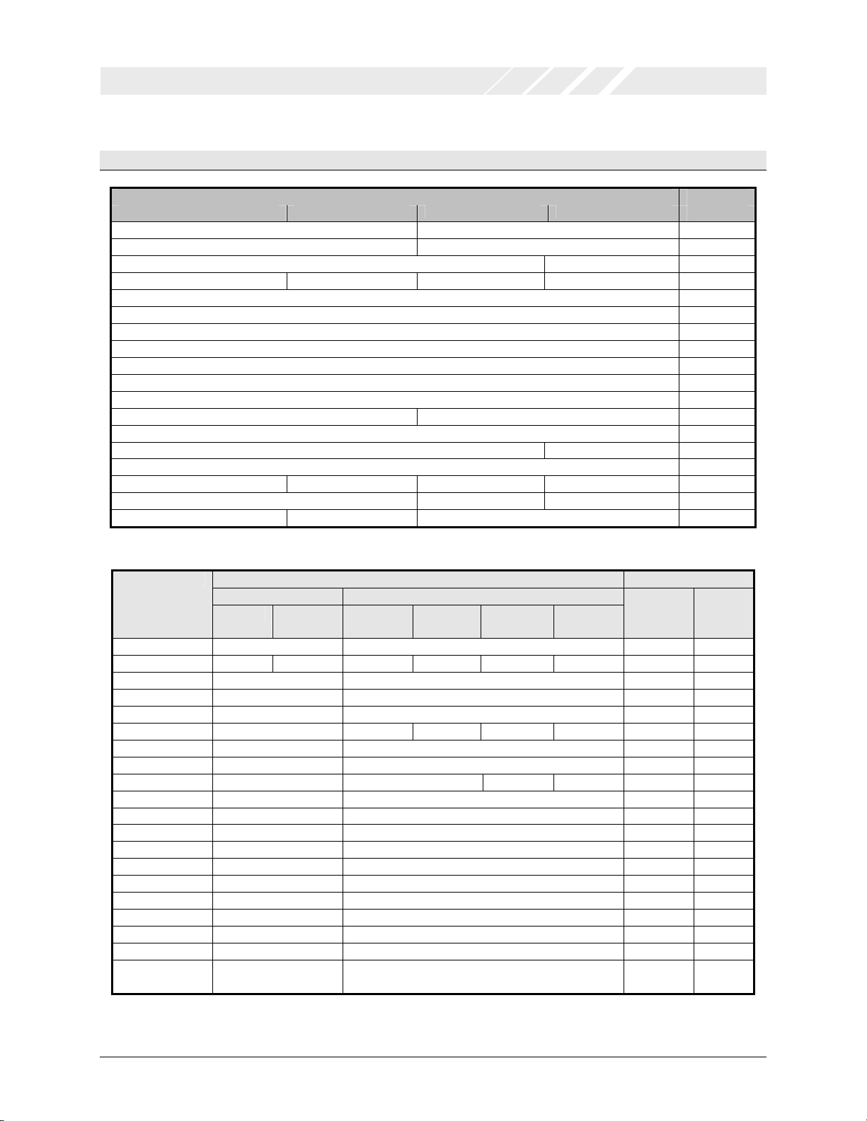
6.2.1 PCI Configura t ion Space Register map
31 16 15 0
Device ID Vendor ID 00h
Status Command 04h
BIST1 Header Type Reserved Reserved 0Ch
Base Address Register 2 (BAR 2) – Local Configuration Registers in IO space 18h
Base Address Register 3 (BAR3) – Local Configuration Registers in Memory space 1Ch
Subsystem ID Subsystem Vendor ID 2Ch
Reserved Reserved Interrupt Pin Interrupt Line 3Ch
Power Management Capabilities (PMC) Next Ptr Cap_ID 40h
Reserved Reserved PMC Control/Status Register (PMCSR) 44h
Configuration Register Description Offset
Class Code Revision ID 08h
Base Address Register 0 (BAR0) 10h
Base Address Register 1 (BAR 1) 14h
Reserved 20h
Reserved 24h
Reserved 28h
Reserved 30h
Reserved Cap_Ptr 34h
Reserved 38h
OX16PCI954
Address
Table 4: PCI Configuration space
Register name
Function 0 Function 1
UARTs Disabled 8-bit bus 32-bit
Vendor ID 0x1415 0x1415 W R
Device ID 0x9501 0x9500 0x9511 0x9512 0x9513 0x9510 W R
Command 0x0000 0x0000 - R/W
Status 0x0290 0x0290 W (bit 4) R/W
Revision ID 0x00 0x00 - R
Class code 0x070006 0x068000 0x068000 0x070101 0x068000 W R
Header type 0x80 0x80 - R
BAR 0 0x00000001 0x00000001 - R/W
BAR 1 0x00000000 0x00000000 00000001 00000000 - R/W
BAR 2 0x00000001 0x00000001 - R/W
BAR 3 0x00000000 0x00000000 - R/W
Subsystem VID 0x1415 0x1415 W R
Subsystem ID 0x0000 0x0000 W R
Cap ptr. 0x40 0x40 - R
Interrupt line 0x00 0x00 - R/W
Interrupt pin 0x01 0x02 W R
Cap ID 0x01 0x01 - R
Next ptr. 0x00 0x00 - R
PM capabilities 0x6C01 0x6C01 W R
PMC control/
status register
0x0000 0x0000 - R/W
Reset value Program read/write
EEPROM PCI
bus
parallel
port
Disabled
Table 5: PCI configuration space default values
DS-0029 Jul 05 External—Free Release Page 16

OXFORD SEMICONDUCTOR LTD.
OX16PCI954
6.3 Accessing logical functions
Access to the UARTs, local bus and parallel port is achieved via standard I/O and memory mapping, at addresses defined by the
Base Address Registers (BARs) in configuration space. The BARs are configured by the system to allocate blocks of I/O and
memory space to the logical functions, according to the size required by the function. The addresses allocated can then be used
to access the functions. The mapping of these BARs is shown inTable 6.
Function 1 BAR Function 0
Local bus Parallel port
0 Internal UARTs (I/O mapped) Local bus (I/O mapped) Parallel port base registers
1 Internal UARTs (memory mapped) Local bus (memory mapped) Parallel port extended registers
2 Local configuration registers (I/O mapped)
3 Local configuration registers (memory mapped)
4 Unused
5 Unused
Table 6: Base Address Register definition
6.3.1 PCI access to internal UARTs
IO and memory space
BAR 0 and BAR 1 of function 0 are used to access the
internal UARTs. The function reserves a 32-byte block of
I/O space and a 4K byte block of memory space. Once the
I/O access enable and Memory access enable bits in the
Command register (configuration space) are set, the
UARTs can be accessed following the mapping shown in
Table 7.
UART
Address
(hex) UART0 UART1 UART2 UART3
000 00 08 10 18
001 01 09 11 19
002 02 0A 12 1A
003 03 0B 13 1B
004 04 0C 14 1C
005 05 0D 15 1D
006 06 0E 16 1E
007 07 0F 17 1F
UART
Address
000 00 20 40 60
001 04 24 44 64
002 08 28 48 68
003 0C 2C 4C 6C
004 10 30 50 70
005 14 34 54 74
006 18 38 58 78
007 1C 3C 5C 7C
Table 7: PCI address map for internal UARTs
Note 1: Since 4K of memory space is reserved and the full bus
PCI Offset from Base Address 0 for
Function0 in IO space (hex)
PCI Offset from Base Address 1 for
Function0 in Memory space (hex)
(I/O and memory)
address is not used for decoding, there are a number of
aliases of the UARTs in the allocated memory region
6.3.2 PCI access to 8-bit local bus
When the local bus is enabled (Mode 00), access to the
bus works in similar fashion to the internal UARTs. The
function reserves a block of I/O space and a block of
memory space. The I/O block size is user definable in the
range of 4 to 256 bytes; the memory range is fixed at 4K
bytes.
I/O space
In order to minimise the usage of IO space, the block size
for BAR0 of Function1 is user definable in the range of 4 to
256 bytes. Having assigned the address range, the user
can define two adjacent address bits to decode up to four
chip selects internally. This facility allows glueless
implementation of the local bus connecting to four external
peripheral chips. The address range and the lower address
bit for chip-select decoding (Lower-Address-CS-Decode)
are defined in the Local Bus Configuration register (see
LT2[26:20] in section 6.4).
The 8-bit Local Bus has eight address lines (LBA[7:0])
which correspond to the maximum IO address space. If the
maximum allowable block size is allocated to the IO space
(i.e. 256 bytes), then as access in IO space is byte aligned,
LBA[7:0] equal PCI AD[7:0] respectively. When the user
selects an address range which is less than 256 bytes, the
corresponding upper address lines will be set to logic zero.
The region can be divided into four chip-select regions
when the user selects the second uppermost non-zero
address bit for chip-select decoding. For example if 32bytes of IO space are reserved, the local bus address lines
A[4:0] are active and the remaining address lines are set to
zero. To generate four chip-selects the user should select
A3 as the Lower-Address-CS-Decode. In this case A[4:3]
will be used internally to decode chip-selects, asserting
LBCS0# when the address offset is 00-07h, LBCS1# when
DS-0029 Jul 05 External—Free Release Page 17
OXFORD SEMICONDUCTOR LTD.
offset is 08-0Fh, LBCS2# when offset is 10-17h, and
LBCS3# when offset is 18- 1Fh.
The region can be divided into two chip-select regions by
selecting the uppermost address bit to decode chip selects.
In the above example, the user can select A4 as the
Lower-Address-CS-Decode, thus using A[5:4] internally to
decode chip selects. As in this example LBA5 is always
zero, only chip-select lines LBCS0# and LBCS1# will be
decoded into, asserting LBCS0# when address offset is 000Fh and LBCS1# when offset is 10-1Fh.
The region can be allocated to a single chip-select region
by assigning an address bit beyond the selected range to
Lower-Address-CS-Decode (but not above A8). In the
above example, if the user selects A5 as the LowerAddress-CS-Decode, A[6:5] will be used to internally
decode chip-selects. As in this example LBA[7:5] are
always zero, only the chip select line LBCS0# may be
selected. In this case address offset 00-1Fh asserts
LBCS0# and the other chip-select lines remain inactive
permanently.
With default values, the address map for local bus IO
address accesses is the same as for internal UARTs.
Memory Space:
The memory base address registers have an allocated
fixed size of 4K bytes in the address space. Since the
Local Bus has 8 address lines and the OX16PCI954 only
implements DWORD aligned accesses in memory space,
the 256 bytes of addressable space per chip select is
expanded to 1K. Unlike an I/O access, for a memory
access the upper address lines are always active and the
internal chip-select decoding logic ignores the user setting
for Lower-Address-CS-Decode (LT2[26:23]) and uses PCI
AD[11:10] to decode into 4 chip-select regions. When the
Local Bus is accessed in memory space, A[9:2] are
asserted on LBA[7:0]. The chip-select regions are defined
below.
Local Bus
Chip-Select
(Data-Strobe)
LBCS0# (LBDS0#) 000h 3FCh
LBCS1# (LBDS1#) 400h 7FCh
LBCS2# (LBDS2#) 800h BFCh
LBCS3# (LBDS3#) C00h FFCh
Table 8: PCI address map for local bus (memory)
Note: The description given for I/O and memory accesses
is for an Intel-type configuration for the Local Bus. For
Motorola-type configuration, the chip select pins are
PCI Offset from BAR 1 in
Function1 (Memory space)
Lower Address Upper Limit
OX16PCI954
redefined to data strobe pins. In this mode the Local Bus
offers up to 8 address lines and four data-strobe pins.
6.3.3 PCI access to parallel port
When the parallel port is enabled (Mode 01), access to the
port works via BAR definitions as usual, except that there
are two I/O BARs corresponding to the two sets of registers
defined to operate an IEEE1284 EPP and bi-directional
Parallel Port.
The user can change the I/O space block size of BAR0 by
over-writing the default values in LT2[25:20] using the
serial EEPROM (see section 6.4). For example the user
can reduce the allocated space for BAR0 to 4-bytes by
setting LT2[22:20] to ‘001’. The I/O block size allocated to
BAR1 is fixed at 8-Bytes.
Legacy parallel ports expect the upper register set to be
mapped 0x400 above the base block, therefore if the BARs
are fixed with this relationship, generic parallel port drivers
can be used to operate the device in all modes.
Example: BAR0 = 0x00000379 (8 bytes at address 0x378)
BAR1 = 0x00000779 (8 bytes at address 0x778)
If this relationship is not used, custom drivers will be
needed.
6.3.4 PCI access to 32-bit local bus
Access to the Local Bus in 32-bit mode is similar to 8-bit
mode (see section 6.3.2) with the following exceptions:
• The local Bus offers a 32-bit bi-directional data bus
and 12 bit address bus
• The PCI address signals ‘AD[13:2]’ are asserted on
LBA[11:0]
• Block size in memory space is programmable by
LT2[28:27] (see section 6.4)
• The Lower-Address-CS-Decode (LT2[26:23])
parameter is used to decode up to 4 chip selects
The block size allocation for chip-select regions is defined
in Table 9.
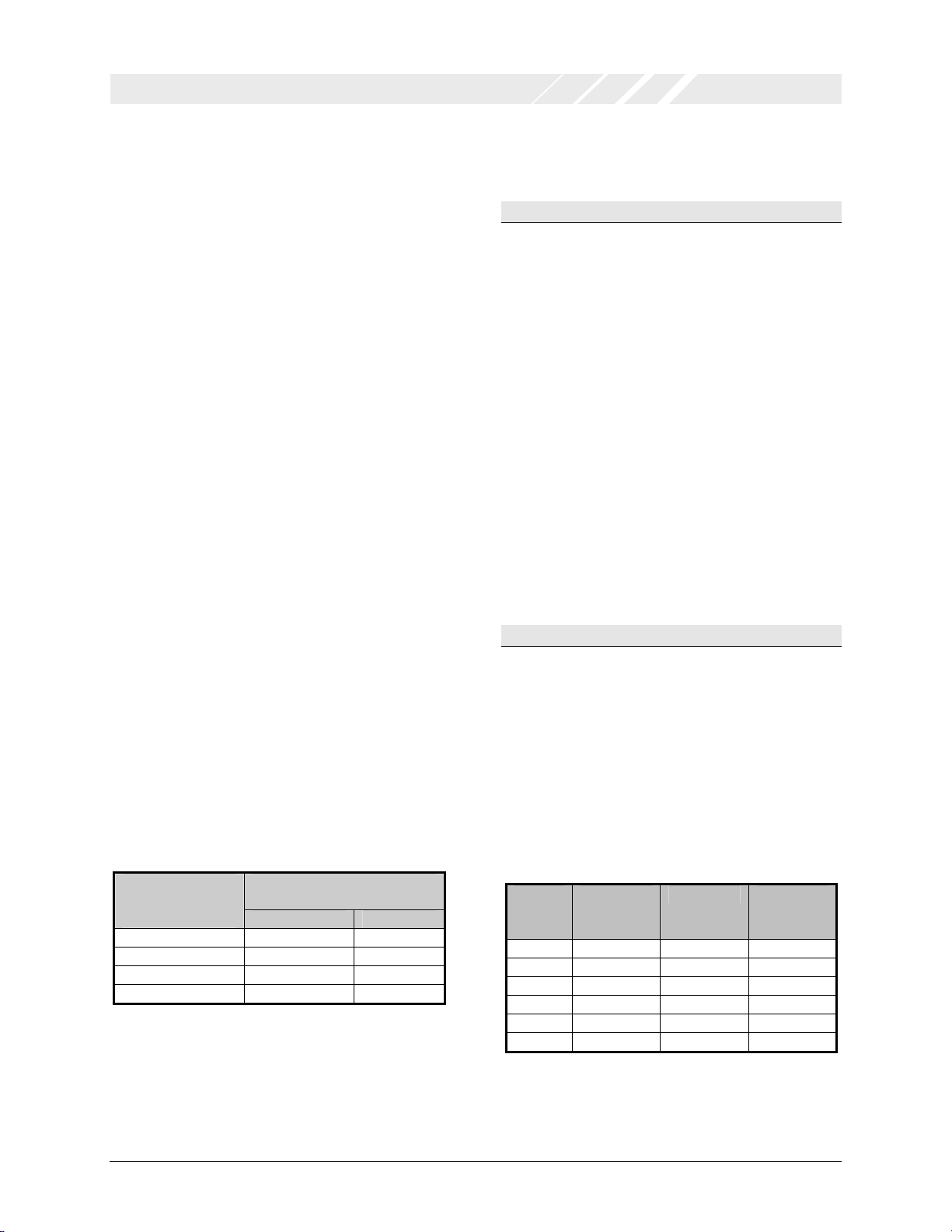
Number
of Chip
selects
1 16 ‘01’ ‘1010’
2 16 ‘01’ ‘1001’
4 16 ‘01’ ‘1000’
1 4 ‘00’ ‘1000’
2 4 ‘00’ ‘0111’
4 4 ‘00’ ‘0110’
Table 9: PCI access to 32-bit local bus (memory)
Memory
block size
(Kbytes)
LT2[28:27] LT2[26:23]
DS-0029 Jul 05 External—Free Release Page 18

OXFORD SEMICONDUCTOR LTD.
OX16PCI954
6.4 Accessing Local configuration registers
The local configuration registers are a set of device specific registers which can be accessed from either function. They are
mapped to the I/O and memory addresses set up in BAR2 and BAR3 of each function, with the offsets defined for each register.
Access is limited to byte only for I/O accesses; memory accesses can also be word or dword accessed, however on little-endian
systems such as Intel 80x86 the byte order will be reversed.
6.4.1 Local Configuration and Control register ‘LCC’ (Offset 0x00)
This register defines control of ancillary functions such as Power Management, external clock reference signals and the serial
EEPROM. The individual bits are described below.
Bits Description Read/Write Reset
1:0 Mode. These bits return the state of the Mode[1:0] pins. - R XX
2 Enable UART clock output. When this bit is set, the buffered UART clock
output pin (UART_CLK_Out) is active. When low UART_CLK_Out is
permanently low.
4:3 Endian Byte-Lane Select for memory access to 8-bit peripherals.
00 = Select Data[7:0] 10 = Select Data[23:16]
01 = Select Data[15:8] 11 = Select Data[31:24]
Memory access to OX16PCI954 is always DWORD aligned. When
accessing 8-bit regions like the internal UARTs, the 8-bit Local Bus and
the parallel port, this option selects the active byte lane. As both PCI and
PC architectures are little endian, the default value will be used by
systems, however, some non-PC architectures may need to select the
byte lane. These bits are ignored in 32-bit Local Bus.
6:5 Power-down filter time. These bits define a value of an internal filter time
for power-down interrupt request in power management circuitry in
Function0. Once Function0 is ready to go into power down mode,
OX16PCI954 will wait for the specified filter time and if Function0 is still
in power-down request mode, it can assert a PCI interrupt (see section
6.6).
00 = power-down request disabled
01 = 4 seconds
7 Function1 MIO2_PME Enable. A value of ‘1’ enables MIO2 pin to set the
PME_Status in PMCSR register, and hence assert the PME# pin if
enabled. A value of ‘0’ disables MIO2 from setting the PME_Status bit
(see section 6.6).
23:8 Reserved. These bits are used for test purposes. The device driver must
write zeros to these bits.
24 EEPROM Clock. For PCI read or write to the EEPROM , toggle this bit to
generate an EEPROM clock (EE_CK pin).
25 EEPROM Chip Select. When 1 the EEPROM chip-select pin EE_CS is
activated (high). When 0 EE_CS is de-active (low).
26 EEPROM Data Out. For writes to the EEPROM, this output bit is the
input-data of the EEPROM. This bit is output on EE_DO and clocked into
the EEPROM by EE_CK.
27 EEPROM Data In. For reads from the EEPROM, this input bit is the
output-data of the EEPROM connected to EE_DI pin.
28 EEPROM Valid. A 1 indicates that a valid EEPROM program is present - R X
29 Reload configur ation from EEPROM. Writing a 1 to this bit re-loads the
configuration from EEPROM. This bit is self-clearing after EEPROM read
30 Reserved - - 0
31 Reserved - R 0
10 = 129 seconds
11 = 518 seconds
EEPROM
W RW 0
W RW 00
W RW 00
W RW 0
- R 0000h
- W 0
- W 0
- W 0
- R X
- W 0
PCI
DS-0029 Jul 05 External—Free Release Page 19

OXFORD SEMICONDUCTOR LTD.
OX16PCI954
6.4.2 Multi-purpose I/O Configuration register ‘MIC’ (Offset 0x04)
This register configures the operation of the multi-purpose I/O pins ‘MIO[11:0] as follows.
Bits Description Read/Write Reset
1:0
3:2 MIO1 Configuration Register (LCC[6:5]=‘00’).
5:4 MIO2 Configuration Register (LCC[7]=’0’).
7:6 MIO3 Configuration Register.
9:8 MIO4 Configuration Register.
11:10 MIO5 Configuration Register.
13:12 MIO6 Configuration Register.
15:14 MIO7 Configuration Register.
MIO0 Configuration Register (Mode[1:0]≠‘01’).
00 -> MIO0 is a non-inverting input pin
01 -> MIO0 is an inverting input pin
10 -> MIO0 is an output pin driving ‘0’
11 -> MIO0 is an output pin driving ‘1’
Unused (Mode[1:0]=‘01’). When Parallel Port is enabled, MIO[0] pin is
unused and will remain in forcing output mode.
00 -> MIO1 is a non-inverting input pin
01 -> MIO1 is an inverting input pin
10 -> MIO1 is an output pin driving ‘0’
11 -> MIO1 is an output pin driving ‘1’
Unused (LCC[6:5] ≠‘00’). When power-down mode in Function0 is
enabled, MIO1 pin is unused and will remain in forcing output mode.
00 -> MIO2 is a non-inverting input pin
01 -> MIO2 is an inverting input pin
10 -> MIO2 is output pin driving ‘0’
11 -> MIO2 is output pin driving ‘1’
PME_Input (LCC[7]=’1’). When LCC[7] is set, MIO2 pin is re-defined to
PME_Input. It’s polarity will be controlled by MIC[4]. It sets the sticky
PME_Status bit in Function1.
00 -> MIO3 is a non-inverting input pin
01 -> MIO3 is an inverting input pin
10 -> MIO3 is an output pin driving ‘0’
11 -> MIO3 is an output pin driving ‘1’
00 -> MIO4 is a non-inverting input pin
01 -> MIO4 is an inverting input pin
10 -> MIO4 is an output pin driving ‘0’
11 -> MIO4 is an output pin driving ‘1’
00 -> MIO5 is a non-inverting input pin
01 -> MIO5 is an inverting input pin
10 -> MIO5 is an output pin driving ‘0’
11 -> MIO5 is an output pin driving ‘1’
00 -> MIO6 is a non-inverting input pin
01 -> MIO6 is an inverting input pin
10 -> MIO6 is an output pin driving ‘0’
11 -> MIO6 is an output pin driving ‘1’
00 -> MIO7 is a non-inverting input pin
01 -> MIO7 is an inverting input pin
10 -> MIO7 is an output pin driving ‘0’
11 -> MIO7 is an output pin driving ‘1’
EEPROM
W RW 00
W RW 00
W RW 00
W RW 00
W RW 00
W RW 00
W RW 00
W RW 00
PCI
DS-0029 Jul 05 External—Free Release Page 20

OXFORD SEMICONDUCTOR LTD.
OX16PCI954
Bits Description Read/Write Reset
17:16 MIO8 Configuration Register.
EEPROM
PCI
W RW 00
00 -> MIO8 is a non-inverting input pin
01 -> MIO8 is an inverting input pin
10 -> MIO8 is an output pin driving ‘0’
11 -> MIO8 is an output pin driving ‘1’
19:18 MIO9 Configuration Register.
W RW 00
00 -> MIO9 is a non-inverting input pin
01 -> MIO9 is an inverting input pin
10 -> MIO9 is an output pin driving ‘0’
11 -> MIO9 is an output pin driving ‘1’
21:20 MIO10 Configuration Register.
W RW 00
00 -> MIO10 is a non-inverting input pin
01 -> MIO10 is an inverting input pin
10 -> MIO10 is an output pin driving ‘0’
11 -> MIO10 is an output pin driving ‘1’
23:22 MIO11 Configuration Register.
W RW 00
00 -> MIO11 is a non-inverting input pin
01 -> MIO11 is an inverting input pin
10 -> MIO11 is an output pin driving ‘0’
11 -> MIO11 is an output pin driving ‘1’
31:24 Reserved - R 00h
6.4.3 Local Bus Timing Parameter register 1 ‘LT1’ (Offset 0x08):
The Local Bus Timing Parameter registers (LT1 and LT2) define the operation and timing parameters used by the Local Bus.
The timing parameters are programmed in 4-bit registers to define the assertion/de-assertion of the Local Bus control signals.
The value programmed in these registers defines the number of PCI clock cycles after a Reference Cycle when the events
occur, where the reference Cycle is defined as two clock cycles after the master asserts the IRDY# signal. The following
arrangement provides a flexible approach for users to define the desired bus timing of their peripheral devices. The timings refer
to I/O or Memory mapped access to BAR0 and BAR1 of Function1.
Bits Description Read/Write Reset
3:0 Read Chip-select Assertion (Intel-type interface). Defines the number of
clock cycles after the Reference Cycle when the LBCS[3:0]# pins are
asserted (low) during a read operation from the Local Bus.
1
These bits are unused in Motorola-type interface.
7:4 Read Chip-select De-assertion (Intel-type interface). Defines the number
of clock cycles after the Reference Cycle when the LBCS[3:0]# pins are
de-asserted (high) during a read from the Local Bus.
1
These bits are unused in Motorola-type interface.
11:8 Write Chip-select Assertion (Intel-type interface). Defines the number of
clock cycles after the Reference Cycle when the LBCS[3:0]# pins are
asserted (low) during a write operation to the Local Bus.
1
These bits are unused in Motorola-type interface.
EEPROM
PCI
W RW 0h
W RW 3h
(2h for
parallel port)
W RW 0h
DS-0029 Jul 05 External—Free Release Page 21

OXFORD SEMICONDUCTOR LTD.
OX16PCI954
Bits Description Read/Write Reset
15:12 Write Chip-select De-assertion (Intel-type interface). Defines the number
of clock cycles after the reference cycle when the LBCS[3:0]# pins are
de-asserted (high) during a write operation to the Local Bus.
1
EEPROM
PCI
W RW 2h
Read-not-Write De-assertion during write cycles (Motorola-type
interface). Defines the number of clock cycles after the reference cycle
when the LBRDWR# pin is de-asserted (high) during a write to the Local
1
Bus.
19:16
Read Control Assertion (Intel-type interface). Defines the number of
clock cycles after the Reference Cycle when the LBRD# pin is asserted
(low) during a read from the Local Bus.
1
W RW 0h
(1h for
parallel port)
Read Data-strobe Assertion (Motorola-type interface). Defines the
number of clock cycles after the Reference Cycle when the LBDS[3:0]#
pins are asserted (low) during a read from the Local Bus.
23:20 Read Control De-assertion (Intel-type interface). Defines the number of
clock cycles after the Reference Cycle when the LBRD# pin is deasserted (high) during a read from the Local Bus.
1
W RW 3h
(2h for
1
parallel port)
Read Data-strobe De-assertion (Motorola-type interface). Defines the
number of clock cycles after the Reference Cycle when the LBDS[3:0]#
pins are de-asserted (high) during a read from the Local Bus.
27:24 Write Control Assertion (Intel-type interface). Defines the number of
clock cycles after the Reference Cycle when the LBWR# pin is asserted
(low) during a write to the Local Bus.
1
1
W RW 0h
(1h for
parallel port)
Write Data-strobe Assertion (Motorola-type interface). Defines the
number of clock cycles after the Reference Cycle when the LBDS[3:0]#
pins are asserted (low) during a write to the Local Bus.
31:28 Write Control De-assertion (Intel-type interface). Defines the number of
1
W RW 2h
clock cycles after the Reference Cycle when the LBWR# pin is deasserted (high) during a write to the Local Bus.
1
Write Data-strobe De-assertion (Motorola-type interface). Defines the
number of clock cycles after the Reference Cycle when the LBDS[3:0]#
pins are de-asserted (high) during a write cycle to the Local Bus.
1
Note 1: Only values in the range of 0h to Ah (0-10 decimal) are valid. Other values are reserved. These parameters apply to both 8-bit and 32-bit Local Bus
configurations. See notes in the following page.
DS-0029 Jul 05 External—Free Release Page 22
 Loading...